* PCBs are custom-made, picture & parameters for reference
High-Performance 4-Layer PCB Solutions with F4BTMS1000 Material for Demanding Applications
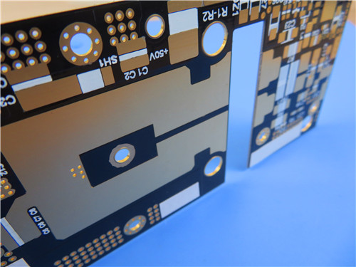
(Custom PCBs are tailored products; the images and specifications provided are for reference only.)
Introduction to F4BTMS1000
The F4BTMS series represents an advanced iteration of the F4BTM series, featuring significant breakthroughs in material formulation and manufacturing processes. This high-reliability material is enriched with a substantial amount of ceramics and reinforced with ultra-thin, ultra-fine glass fiber cloth, resulting in enhanced performance and a broader range of dielectric constants. It is particularly suitable for aerospace applications and can effectively replace comparable foreign products.
By incorporating a carefully balanced mix of ultra-thin glass fiber cloth and specially distributed nano-ceramics combined with polytetrafluoroethylene resin, the negative impacts of glass fiber on electromagnetic wave propagation are minimized. This innovation reduces dielectric loss, enhances dimensional stability, and decreases anisotropy in the X/Y/Z axes. Additionally, it improves electrical strength, thermal conductivity, and exhibits excellent low thermal expansion characteristics.
Properties of F4BTMS1000
Dielectric Constant (Dk): 10.2 at 10 GHz
Dissipation Factor: 0.0020 at 10 GHz, 0.0023 at 20 GHz
Coefficient of Thermal Expansion (CTE):
X-axis: 16 ppm/°C
Y-axis: 18 ppm/°C
Z-axis: 32 ppm/°C (from -55°C to 288°C)
Low Thermal Coefficient of Dk: -320 ppm/°C (from -55°C to 150°C)
High Thermal Conductivity: 0.81 W/mK
Low Moisture Absorption: 0.03%
PCB Construction Details
| Specification | Details |
|---|---|
| Base Material | F4BTMS1000 |
| Layer Count | 4 layers |
| Board Dimensions | 145mm x 145mm (± 0.15mm) |
| Minimum Trace/Space | 5/7 mils |
| Minimum Hole Size | 1.2mm |
| Blind Vias | Top to Inner Layer 1; Buried: Inner Layer 2 to Inner Layer 3 |
| Finished Board Thickness | 12.9mm |
| Finished Copper Weight | 1 oz (1.4 mils) for inner and outer layers |
| Via Plating Thickness | 20 µm |
| Surface Finish | HASL (Hot Air Solder Leveling) |
| Top Silkscreen | White |
| Bottom Silkscreen | No |
| Top Solder Mask | Black |
| Bottom Solder Mask | No |
| Electrical Testing | 100% Electrical Testing conducted prior to shipment |
PCB Stackup
Copper Layer 1: 35 µm
F4BTMS1000 Core: 6.35 mm (250 mil)
Copper Layer 2: 35 µm
Prepreg RO4450F: 0.102 mm (4 mil)
Copper Layer 3: 35 µm
F4BTMS1000 Core: 6.35 mm (250 mil)
Copper Layer 4: 35 µm
PCB Statistics
Components: 19
Total Pads: 77
Through Hole Pads: 35
Top SMT Pads: 42
Bottom SMT Pads: 0
Vias: 32
Nets: 2
Artwork and Standards Information
Type of Artwork Supplied: Gerber RS-274-X
Accepted Standard: IPC-Class-2
Availability: Worldwide
Typical Applications
Aerospace equipment and cabin systems
Microwave and RF applications
Military radar systems
Feed networks
Phase-sensitive and phased array antennas
Satellite communications and more
Get a Quick Quote
Fill in the form below and our engineers will reply within 24 hours with technical specifications and pricing for F4BTMS1000 4-Layer High-Performance PCB.


