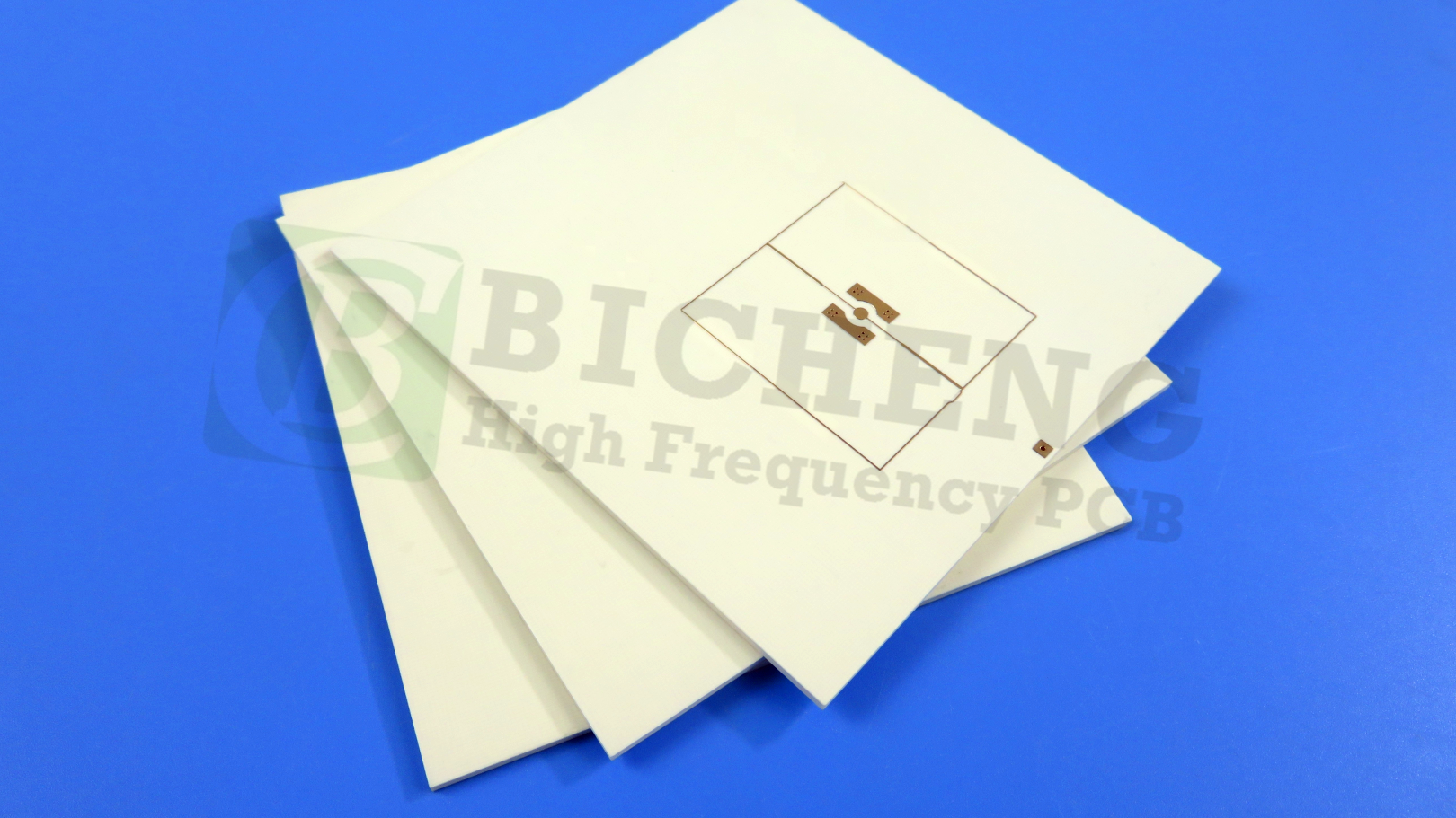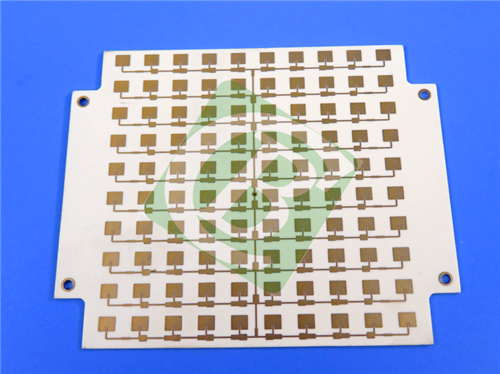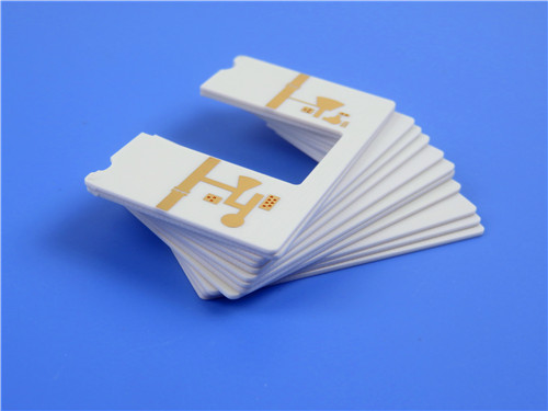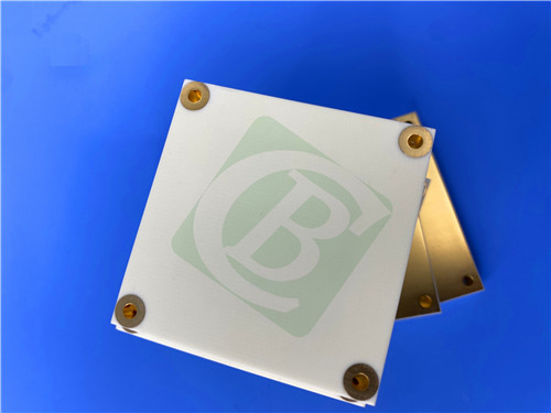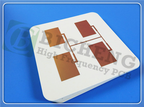
RO4003C Multilayer PCB 4-Layer 4.8mm Thick Low Loss Material for Microstrip and Stripline Circuits1.Introduction to RO4003C Rogers RO4003C materials are advanced woven glass reinforced hydrocarbon/ceramic composites that combine the electrical performance characteristics of PTFE/woven glass with the manufacturability of epoxy/glass. This innovative design provides superior high-frequency performance and facilitates low-cost circuit fabrication. The result is a low-loss material that can be produced using standard epoxy/glass (FR-4) processes, all at competitive prices. RO4003C materials are ideal for RF microwave circuit designers and are particularly suited for matching networks and controlled impedance transmission lines. The low dielectric loss of RO4003C allows it to be utilized in many applications where conventional circuit board laminates are limited by higher operating frequencies. Available in various configurations, RO4003C laminates are manufactured using both 1080 and 1674 glass fabric styles, ensuring that all configurations meet the same electrical performance specifications. Importantly, RO4003C materials are non-brominated and do not carry a UL 94 V-0 rating. 2.Features of RO4003C Dielectric Constant: DK 3.38 ± 0.05 at 10 GHz 3.PCB Stackup: 4-Layer Rigid PCB Copper Layer 1: 35 µm
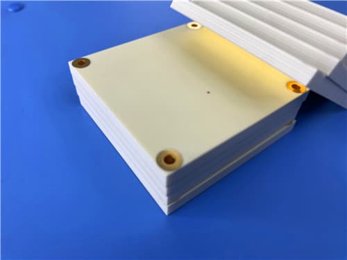
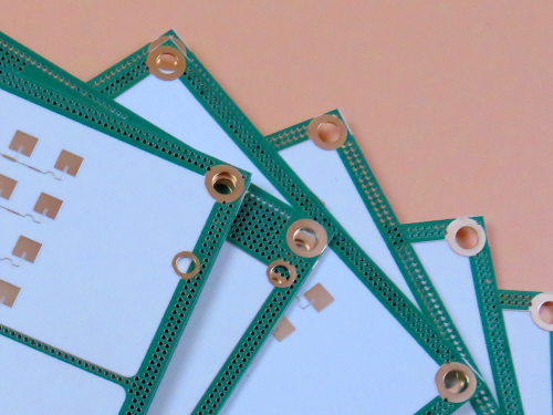
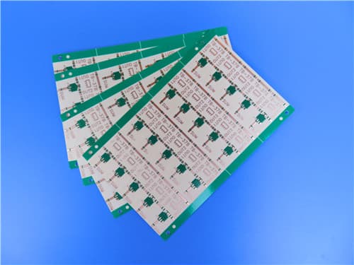
4.PCB Construction Details Board Dimensions: 65 mm x 65 mm (1 piece), ± 0.15 mm 5.PCB Statistics Components: 6 6.Artwork and Standards Type of Artwork Supplied: Gerber RS-274-X 7.Typical Applications Commercial airline broadband antennas |
Get a Quick Quote
Fill in the form below and our engineers will reply within 24 hours with technical specifications and pricing for Rogers RO4003C Multilayer PCB 4-Layer 4.8mm Thick Low Loss Material for Microstrip and Stripline Circuits.