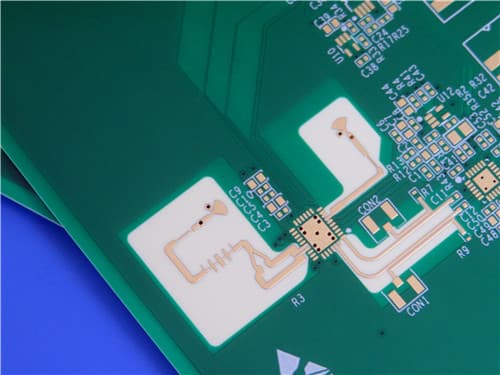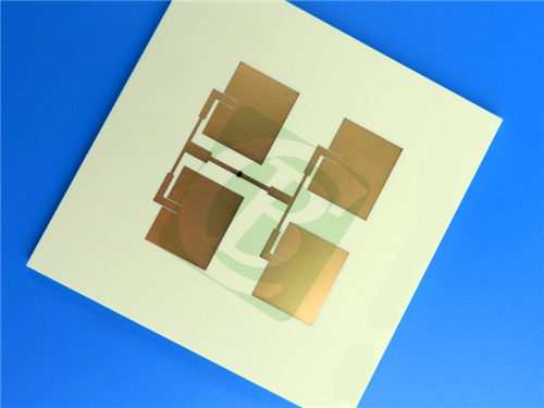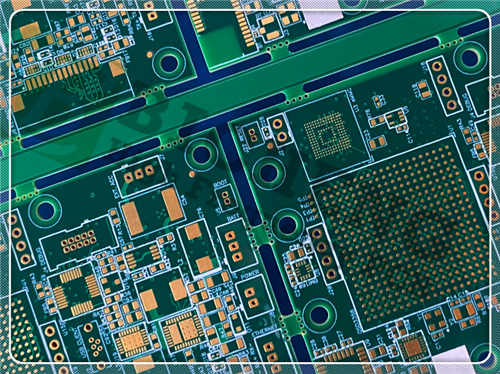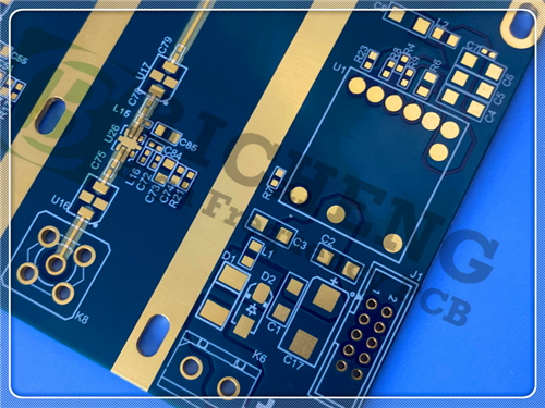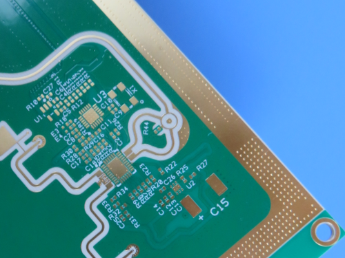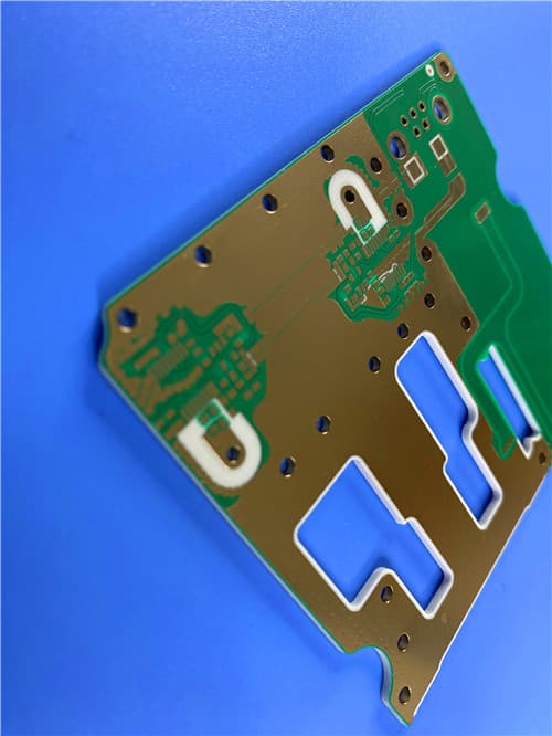
* PCBs are custom-made, picture & parameters for reference
RO4003C + RO4450F 4-Layer Hybrid PCB with Resin-Plugged Vias & IPC-6012 Class 3 for RF & Microwave Applications1. Introduction to RO4003C + RO4450F 4-Layer Hybrid PCB Rogers RO4003C™ is a ceramic-filled hydrocarbon laminate designed for high-frequency applications. It offers a stable dielectric constant of 3.38 ± 0.05 at 10GHz and a low dissipation factor of 0.0027, making it ideal for RF and microwave circuits. RO4450F™ is a compatible prepreg system used for multi-layer bonding, providing excellent flow and adhesion characteristics. RO4003C and RO4350B laminates are compatible with many thermosetting and thermoplastic adhesive systems. These materials are compatible with standard FR-4 processing, including standard drilling, plating, and routing techniques. They do not require any special through hole treatments commonly needed when processing PTFE-based laminate materials. This 4-layer rigid PCB is constructed with two 0.203mm RO4003C cores and two layers of RO4450F prepreg (total 0.204mm), finished at 0.75mm thickness. All layers have 1oz copper, with top green solder mask and white legend, bottom green mask no legend. The surface finish is ENIG 2u". All vias are resin-plugged and electroplated filled, with 25μm IPC-6012 Class 3 plated copper for high reliability.
2. Key Features
3. Benefits
4. PCB Construction Details
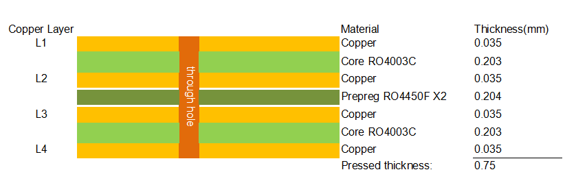
5. PCB Stackup (4-Layer Hybrid Structure) Layer 1 (Top): Copper, 35 μm (1 oz) Dielectric: RO4003C Core, 0.203 mm Layer 2 (Inner): Copper, 35 μm (1 oz) Prepreg: RO4450F x 2, total 0.204 mm Layer 3 (Inner): Copper, 35 μm (1 oz) Dielectric: RO4003C Core, 0.203 mm Layer 4 (Bottom): Copper, 35 μm (1 oz) Total thickness: 0.75 mm
6. Resin-Plugged Via Specification
7. RO4003C/RO4350B/RO4835 Circuit Processing Guidelines Storage: Fully clad RO4003C, RO4350B and RO4835 laminates should be stored at room temperature (between 50-90°F/10-32°C). A first-in-first-out inventory system and a method to track material lot numbers through PWB processing and delivery of finished circuits is recommended. Inner Layer Preparation: RO4003C, RO4350B and RO4835 laminates are compatible with many pinned and pinless tooling systems. Choosing whether to use round or slotted pins, external or internal pinning, standard or multiline tooling, and pre vs. post-etch punching would depend on the capabilities and preferences of the circuit facility and final registration requirements. In general, slotted pins, a multiline tooling format, and post-etch punching will meet most needs. Surface Preparation for Photoresist Processing and Copper Etching: Depending upon RO4003C, RO4350B and RO4835 core thickness, copper surfaces can be prepared for photo imaging using chemical or mechanical processes. Thinner cores should be prepared using a chemical process consisting of cleaning, micro-etching, water rinsing, and drying steps. Thicker RO4003C, RO4350B and RO4835 cores are compatible with mechanical scrub systems. RO4003C, RO4350B and RO4835 materials are compatible with most liquid and dry film photo-resists and, once patterned, can be processed through develop, etch, and strip (DES) systems typically used to process FR-4 materials. Oxide Treatment: RO4003C, RO4350B and RO4835 cores can be processed through any copper oxide or oxide alternative process in preparation for multi-layer bonding. The best treatment choice is typically the one recommended in the guidelines supporting the chosen prepreg or adhesive system. Multi-Layer Bonding: RO4003C, RO4350B and RO4835 laminates are compatible with many thermosetting and thermoplastic adhesive systems. Guidelines for the adhesive system should be consulted for bond cycle parameters. Drilling Considerations: Standard entry (aluminum or thin pressed phenolic) and exit (pressed phenolic or fiber board) materials can be used when drilling RO4003C, RO4350B and RO4835 cores or bonded assemblies in one-up or multi-up stacks. RO4003C, RO4350B and RO4835 materials are compatible with a broad range of drilling parameters. However, drilling speeds greater than 500 surface feet per minute (SFM) should be avoided. Chip loads greater than 0.002"/rev are recommended for mid-range and large diameter tools while lower chiploads (<0.002"/rev) are recommended for small (<0.0135") diameter drills. Recommended Drilling Parameters:
Drilling Quick Reference Table:
*Conditions stated are tapered from 200 SFM and 0.002" chip load up to 400 SFM and 0.003" chip load. PTH Processing: Thick multi-layer and double-sided constructions can be processed through conveyorized debur equipment that uses oscillating nylon brushes to abrade the copper surfaces. Thinner layers may require pumice scrubbing by hand, conveyorized processing with an abrasive spray, or chemical preparation. Desmear is typically not required of drilled holes in double-sided boards as the high glass transition temperature of the resin system (>280°C/>536°F) minimizes the occurrence of smear. Multi-layer boards may require desmear depending upon the needs of the bondply or prepreg layers. If desmear is required, a single or double pass through alkaline permanganate or a CF4/O2 plasma process may be used. Metal Deposition: RO4003C, RO4350B and RO4835 materials do not require special treatments prior to metallization and are compatible with electroless copper processing and direct deposition of ionic and colloidal conductive layers. A copper flash plate (0.00025") prior to imaging might be considered for boards with high aspect ratio holes. Copper Plating & Outer-Layer Processing: RO4003C, RO4350B and RO4835 laminates are compatible with panel and pattern processing using standard acid copper and electrolytic tin or tin/lead plating. Once plated, RO4003C, RO4350B and RO4835 laminates can be processed through any standard strip/etch/strip (SES) process. The post-etch surface of RO4003C, RO4350B and RO4835 laminates should be preserved as this surface will bond very well with direct screened and photo-imageable solder masks. Final Metal Finishes: RO4003C, RO4350B and RO4835 laminates are compatible with organic solderability preservatives (OSP's), hot air solder levelling (HASL), and most chemically deposited or electroplated finishes. Routing: RO4003C, RO4350B and RO4835 laminates are routed using carbide tools and conditions that are typical to processing traditional epoxy/glass materials. Copper should be etched away from the routing path to prevent burring. Maximum Stack Height: The maximum stack height should be based on 70% of the actual flute length to allow for debris removal. Routing Quick Reference Table:
Shelf Life: Rogers' High Frequency laminates can be stored for extended durations under ambient room temperatures (55-85°F, 13-30°C) and humidity levels. At room temperature, the dielectric materials are inert to high humidity. However, metal claddings such as copper can be oxidized during exposure to high humidity. (Oxidation on the copper surface can easily be removed in a standard micro-etch process.) In addition, over an extended period (>5 years) the exposed dielectric along edges of the panel may experience detectable levels of oxidation. Accounting for standard tooling hole and trim loss, such trace levels of oxidation would not be expected to extend into the utilized portion of the laminate. Data Source Notes: Prolonged exposure in an oxidative environment may cause changes to the dielectric properties of hydrocarbon based materials. The rate of change increases at higher temperatures and is highly dependent on the circuit design. Although Rogers' high frequency materials have been used successfully in innumerable applications and reports of oxidation resulting in performance problems are extremely rare, Rogers recommends that the customer evaluate each material and design combination to determine fitness for use over the entire life of the end product. Quality Assurance
8. RO4003C/RO4350B/RO4835 Material Features Summary
|
Get a Quick Quote
Fill in the form below and our engineers will reply within 24 hours with technical specifications and pricing for RO4003C + RO4450F 4-Layer Hybrid PCB.