RO4350B and S1000-2M High-Performance PCB Design – Ideal for RF, Radar, and Millimeter-Wave Applications1. Introduction of RO4350B Rogers RO4350B materials are proprietary woven glass-reinforced hydrocarbon/ceramics that offer electrical performance comparable to PTFE/woven glass while maintaining the manufacturability of epoxy/glass. RO4350B laminates provide precise control over dielectric constant (Dk) and low loss, utilizing standard epoxy/glass processing methods. They are cost-effective compared to conventional microwave laminates and do not require special handling procedures. These materials are UL 94 V-0 rated, suitable for high power RF designs. The thermal coefficient of expansion (CTE) of RO4350B is similar to copper, ensuring excellent dimensional stability crucial for mixed dielectric multi-layer board constructions. The low Z-axis CTE guarantees reliable plated through-hole quality, even under severe thermal shock. The material has a Tg of >280°C (536°F), ensuring stable expansion characteristics throughout circuit processing temperatures. 2.Key Features: (1).Features of RO4350B Dielectric Constant of DK 3.48 ±0.05 at 10GHz/23°C
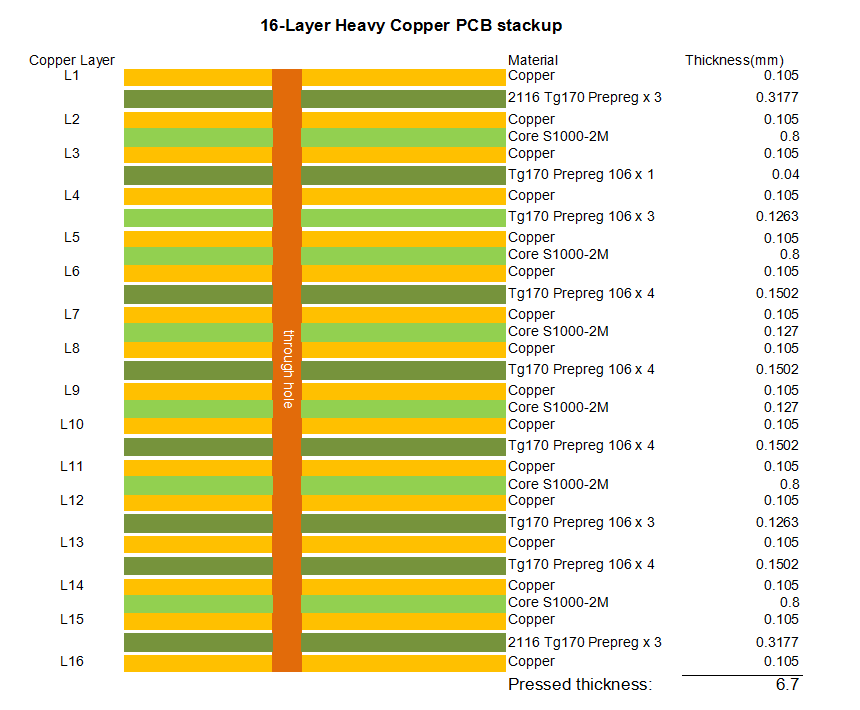
(2).Features of S1000-2M Lower Z-axis CTE for improved through-hole reliability 3.PCB Stackup: 4-layer rigid PCB
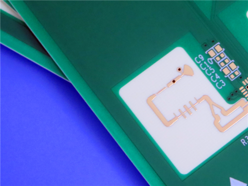
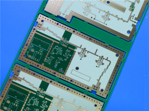
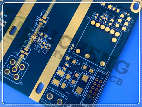
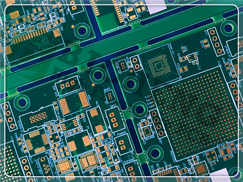
4.PCB Construction Details
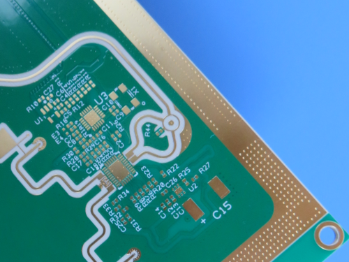
5.PCB Statistics Components: 33 6.Accepted Standards Artwork Format: Gerber RS-274-X 7.Typical Applications Commercial airline broadband antennas |
Get a Quick Quote
Fill in the form below and our engineers will reply within 24 hours with technical specifications and pricing for RO4350B and S1000-2M High-Performance PCB Design – Ideal for RF, Radar, and Millimeter-Wave Applications.
.jpg)
.jpg)
