Rogers RO4003C 6-Layer PCB with Back Drilling and ENIG Finish
1.Introduction to Core Technologies
RO4003C is a high-performance hydrocarbon ceramic laminate developed by Rogers Corporation, specifically designed for RF and microwave applications. It offers a unique combination of low loss, stable electrical properties, and standard epoxy/FR-4 fabrication processes. Unlike traditional PTFE-based materials, RO4003C does not require specialized plasma treatment or sodium etch for through-hole preparation, making it cost-effective and manufacturing-friendly.
2.RO4003C Key Features and Benefits
Stable Dk 3.38 ± 0.05 at 10 GHz ensures consistent impedance control across frequency and temperature
Low Df 0.0027 at 10 GHz minimizes signal loss for high-frequency circuits
Tg >280°C and Td 425°C provide excellent thermal reliability for lead-free assembly
CTE 14-16 ppm/°C (X/Y) matches copper for superior dimensional stability in multilayer designs
Moisture absorption only 0.06% maintains electrical performance in humid environments
UL 94 V-0 rated for safety compliance
Compatible with standard epoxy/FR-4 fabrication eliminates need for plasma treatment, reducing manufacturing cost
Cost-effective alternative to PTFE materials enables high-volume commercial applications
Proven reliability in wireless communications, automotive radar, and aerospace systems
3.What is Back Drilling?
Back drilling is a PCB manufacturing process that removes the unused portion of plated through-hole stubs that extend beyond the last connected layer. These stubs act as antennas and cause signal reflections, impedance discontinuities, and resonance in high-speed and high-frequency circuits. By drilling out these stubs with a larger diameter bit, back drilling improves signal integrity, reduces insertion loss, and minimizes jitter for high-speed digital and RF signals.
4.RO4003C Data Sheet Summary
| Property |
Conditions |
Typical Value |
Unit |
Test Method |
| Dielectric Constant (Dk) | @ 10 GHz | 3.38 ± 0.05 | - | IPC-TM-650 2.5.5.5 |
| Dissipation Factor (Df) | @ 10 GHz | 0.0027 | - | IPC-TM-650 2.5.5.5 |
| Thermal Conductivity | 80°C | 0.71 | W/m·K | ASTM D5470 |
| Tg (Glass Transition) | DMA | >280 | °C | IPC-TM-650 2.4.24 |
| Td (Decomposition Temp) | 5% weight loss | 425 | °C | IPC-TM-650 2.4.24.6 |
| CTE - X/Y axis | -55 to 288°C | 14-16 | ppm/°C | IPC-TM-650 2.4.41 |
| CTE - Z axis | -55 to 288°C | 46 | ppm/°C | IPC-TM-650 2.4.41 |
| Volume Resistivity | C96/35/90 | 1.7 x 10¹⁰ | MΩ-cm | IPC-TM-650 2.5.17.1 |
| Surface Resistivity | C96/35/90 | 4.2 x 10⁹ | MΩ | IPC-TM-650 2.5.17.1 |
| Flexural Strength | LW/CW | 276/213 | MPa | IPC-TM-650 2.4.4 |
| Copper Peel Strength | 1 oz after solder | 1.05 | N/mm | IPC-TM-650 2.4.8 |
| Moisture Absorption | D48/50 | 0.06 | % | IPC-TM-650 2.6.2.1 |
| Flammability Rating | UL94 | V-0 | - | UL 94 |
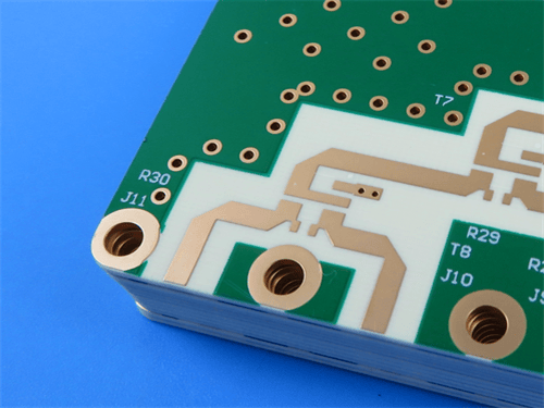
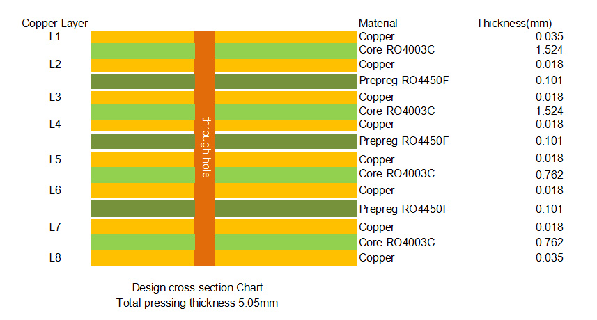
5.PCB Specifications
| Item |
Specification |
| Product Type | 6-Layer High-Frequency PCB |
| Core Material | Rogers RO4003C (0.203mm each) |
| Prepreg Material | Rogers RO4450F |
| Layer Count | 6 Layers |
| Outer Layer Copper | 1oz (approx. 35μm) |
| Inner Layer Copper | 0.5oz (approx. 18μm) |
| Finished Thickness | 1.174mm |
| Surface Finish | ENIG (Electroless Nickel Immersion Gold) |
| Solder Mask | Green (Top and Bottom) |
| Silkscreen | White (Top and Bottom) |
| Special Process | Back Drilling L1-L3, L1-L5 |
| Dimensions | 92.5mm x 77.3mm = 1 PCS |
6.PCB Stackup (6-Layer Rigid Structure)
L1 (Top): 1oz Copper
Core: RO4003C, 0.203mm
L2: 0.5oz Copper
Prepreg: RO4450F (2 sheets), total 0.202mm
L3: 0.5oz Copper
Core: RO4003C, 0.203mm
L4: 0.5oz Copper
Prepreg: RO4450F (2 sheets), total 0.202mm
L5: 0.5oz Copper
Core: RO4003C, 0.203mm
L6 (Bottom): 1oz Copper
7.Typical Applications
Wireless Communications: Base stations, antennas, power amplifiers
Automotive Radar: 77GHz ADAS sensors
Aerospace & Defense: Radar systems, avionics, satellite communications
Test & Measurement: RF test equipment, network analyzers
8.Quality Assurance
Artwork Format: Gerber RS-274-X
Quality Standard: IPC-Class-2
Availability: Worldwide
|

.jpg)