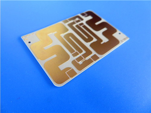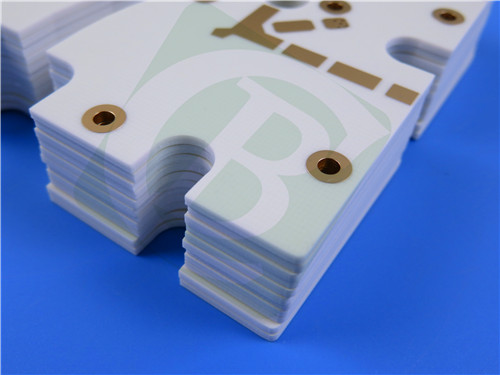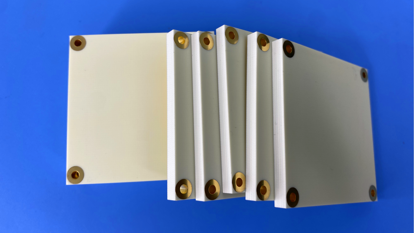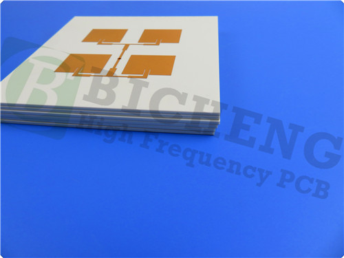
TFA294 PCB 2-Layer 0.127mm Thick High-Frequency PTFE Ceramic Composites for Aerospace Applications1.Introduction of TFA Series The TFA series features a dielectric layer made from a Polytetrafluoroethylene (PTFE) ceramic composite. Unlike traditional methods that involve impregnating glass fiber cloth with resin to create prefabricated sheets, this series employs a unique process to produce these sheets, which are then pressed using a specialized lamination technique. The resulting material showcases exceptional electrical, thermal, and mechanical properties, providing an aerospace-grade, high-frequency, and highly reliable alternative to similar foreign products. This substrate series is free of glass fiber cloth and incorporates a significant amount of uniform special nano-ceramics blended with resin. This design removes the fiberglass effect during electromagnetic wave propagation, leading to outstanding frequency stability and minimal dielectric loss. Additionally, the material exhibits reduced X/Y/Z anisotropy and features a low thermal expansion coefficient comparable to that of copper foil, along with stable dielectric temperature characteristics. The dielectric constant options available in this series are 2.94, 3.0, 6.15, and 10.2, corresponding to part numbers TFA294, TFA300, TFA615, and TFA1020. 2.Features (TFA294) Dielectric constant (Dk) of 2.94 at 10 GHz
3.PCB Stackup: 2-layer rigid PCB 4.PCB Construction Detail Board dimensions: 58.1 mm x 66 mm (1 piece, +/- 0.15 mm) 5.PCB Statistics 6.Type of Artwork Supplied: 7.Quality Standard: 8. Availability: 9. Some Typical Applications Aerospace equipment, including in-cabin systems and aircraft |
Get a Quick Quote
Fill in the form below and our engineers will reply within 24 hours with technical specifications and pricing for TFA294 PCB 2-Layer 0.127mm Thick High-Frequency PTFE Ceramic Composites for Aerospace Applications.