| |
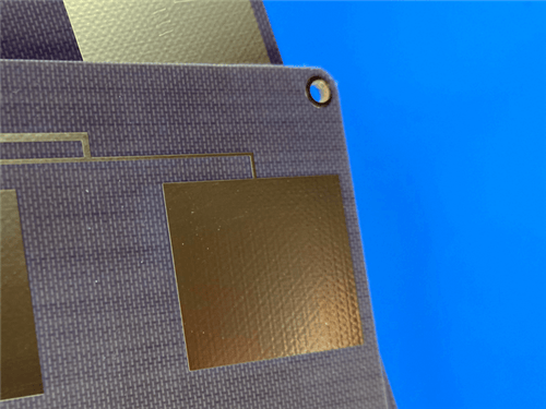
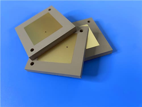
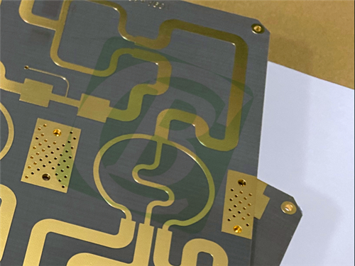
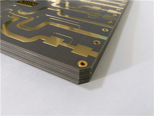
Wangling TP2000 2-Layer 6.1mm Bare Copper PCB for High-DK RF & Antenna Applications
1.Introduction to TP2000 PCB
TP2000 material is a unique high frequency thermoplastic material in the industry. The dielectric layer of TP based sheets is composed of ceramic and polyphenylene oxide (PPO) resin, with no glass fiber reinforcement, engineered for high-frequency RF and microwave applications. It features an ultra-high dielectric constant, ultra-low dissipation factor, and excellent thermal stability, making it ideal for designs requiring compact size and high signal integrity. The material operates reliably across a wide temperature range and is easy to machine, supporting standard PCB fabrication processes.
This 2-layer rigid PCB is constructed entirely with TP2000 as the core material, providing exceptional signal integrity, compact design capability due to high DK, and thermal stability for demanding RF, microwave, and aerospace applications.
2.Key Features of TP2000
Dielectric Constant (DK): 20 at 5GHz Dissipation Factor (Df): 0.002 at 5GHz Thermal Coefficient of DK (TCDK): -55 ppm/°C Coefficient of Thermal Expansion (CTE): X=35 ppm/°C, Y=35 ppm/°C, Z=40 ppm/°C Operating Temperature Range: -100°C to +150°C High mechanical strength and dimensional stability Excellent radiation resistance Easy machinability (drilling, cutting, engraving) Compatible with standard PCB assembly processes UL 94-V0 flammability rating
3.Benefits of TP2000 PCB
Ultra-high dielectric constant enables circuit miniaturization Ultra-low dissipation factor for excellent signal integrity Excellent thermal stability across wide temperature range (-100°C to +150°C) No glass fiber reinforcement – homogeneous dielectric properties Excellent radiation resistance for aerospace and defense applications Easy machinability – can be drilled, cut, and engraved Compatible with standard PCB assembly processes High mechanical strength and dimensional stability
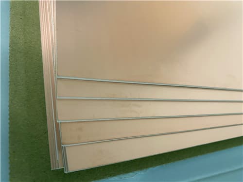
4.TP2000 PCB Construction Details
| Item | Specification |
|---|
| Base material | TP2000 |
| Layer count | 2 layers |
| Board dimensions | 85mm x 85mm = 1PCS, +/- 0.15mm |
| Minimum Trace/Space | 6/7 mils |
| Minimum Hole Size | 0.35mm |
| Blind vias | No |
| Finished board thickness | 6.1mm |
| Finished Cu weight | 1 oz (1.4 mils) outer layers |
| Via plating thickness | 20 μm |
| Surface finish | Bare copper |
| Top Silkscreen | No |
| Bottom Silkscreen | No |
| Top Solder Mask | No |
| Bottom Solder Mask | No |
| 100% Electrical test | Used prior to shipment |
5.PCB Stackup (2-Layer Rigid Structure)
Copper_layer_1 – 35 μm
TP2000 core – 6 mm
Copper_layer_2 – 35 μm
6.PCB Statistics
Components: 24
Total Pads: 37
Thru Hole Pads: 18
Top SMT Pads: 19
Bottom SMT Pads: 0
Vias: 12
Nets: 2
7.Primary Application Areas
High-frequency RF and microwave circuits Antenna systems (including phased array antennas) Radar systems (automotive, aerospace, defense) Satellite communication equipment High-power RF amplifiers Test and measurement instruments Aerospace and defense electronics
8.Quality Assurance
Artwork supplied: Gerber RS-274-X
Accepted standard: IPC-Class-2
Availability: Worldwide
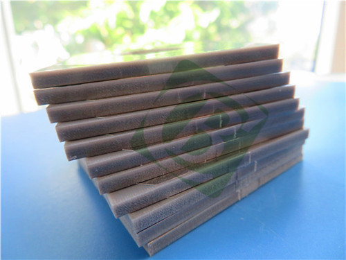
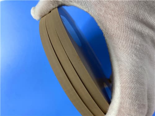
9.TP2000 Microwave Composite Copper-Clad Laminate – Product Introduction
TP material is a unique high frequency thermoplastic material in the industry. The dielectric layer of TP based sheets is composed of ceramic and polyphenylene oxide (PPO) resin, with no glass fiber reinforcement. The dielectric constant is precisely adjusted by controlling the ratio between ceramic and PPO resin. The production process is special, resulting in excellent dielectric properties and high reliability.
TP refers to unclad smooth surface material, TP-1 refers to single-sided copper clad material, and TP-2 refers to double-sided copper clad material.
10.Features and Benefits
Key Features
Dielectric constant can be arbitrarily selected within the range of 3 to 25 according to circuit requirements, with stable performance. Common dielectric constants include 3.0, 4.4, 6.0, 6.15, 9.2, 9.6, 10.2, 11, 16, 20. Low dielectric loss – loss increases with frequency, but changes little within 10GHz. Long-term operating temperature range: -100°C to +150°C. Excellent low-temperature resistance. When temperature exceeds 180°C, the material may deform, copper foil may detach, and electrical properties may change significantly. Minimum thickness 0.5mm, rich thickness options, customizable. Radiation resistant and low outgassing. Ideal material for Beidou navigation, missile-borne systems, fuzes, and miniaturized antennas. Adhesion between copper foil and dielectric is stronger than vacuum coating on ceramic substrates. Material is easy to machine – can be drilled, turned, ground, sheared, engraved, etc. – which ceramic substrates cannot match. Easy PCB processing using standard thermoplastic material processing methods. High yield rate and significantly lower processing cost compared to ceramic substrates. Due to material characteristics, multi-layer processing is generally not recommended. If multi-layer processing is required, please select low-temperature bonding sheets and fully consider feasibility. Material is not suitable for 260°C thermal shock testing and cannot undergo wave soldering. Soldering recommendation: manual soldering with constant temperature iron. Reflow soldering is generally not recommended. If reflow soldering is required, the maximum set temperature should not exceed 200°C, and feasibility and stability should be fully considered.
Benefits
Ultra-high dielectric constant enables circuit miniaturization Ultra-low dissipation factor for excellent signal integrity Excellent thermal stability across wide temperature range (-100°C to +150°C) No glass fiber reinforcement – homogeneous dielectric properties Excellent radiation resistance for aerospace and defense applications Easy machinability – can be drilled, cut, and engraved Compatible with standard PCB assembly processes High mechanical strength and dimensional stability
11.TP2000 Data Sheet
| Property | Test Condition | Units | TP2000 Typical Value |
|---|
| Dielectric Constant | 5 GHz | – | 20.0 ± 0.8 |
| Dielectric Constant Range | – | – | Customizable from 3.0 to 25 |
| Dielectric Constant Tolerance | – | % | ±4% |
| Dissipation Factor | 5 GHz | – | 0.0020 – 0.0025 |
| Temperature Coefficient of Dk | -55°C to 150°C | ppm/°C | -55 |
| Peel Strength (1 oz, Normal State) | – | N/mm | >0.6 |
| Peel Strength (1 oz, After Damp Heat) | – | N/mm | >0.4 |
| Volume Resistivity | Normal State, 500V | Mohm·cm | >1 × 10⁹ |
| Surface Resistivity | Normal State, 500V | Mohm | >1 × 10⁷ |
| CTE (X axis, -55°C to 150°C) | – | ppm/°C | 35 |
| CTE (Y axis, -55°C to 150°C) | – | ppm/°C | 35 |
| CTE (Z axis, -55°C to 150°C) | – | ppm/°C | 40 |
| Moisture Absorption | 20±2°C, 24 hours | % | ≤0.01 |
| Long-Term Operating Temperature | – | °C | -100 to +150 |
| Density | – | g/cm³ | 2.73 |
| Thermal Conductivity | – | W/(m·K) | 0.85 |
| Material Composition | – | – | PPO + Ceramic + ED Copper |
| Flammability Rating | UL-94 | Class | V-0 |
12.Some Typical Applications
High-frequency RF and microwave circuits Antenna systems (including phased array antennas) Radar systems (automotive, aerospace, defense) Satellite communication equipment High-power RF amplifiers Test and measurement instruments Aerospace and defense electronics Beidou navigation systems Missile-borne systems Fuzes Miniaturized antennas
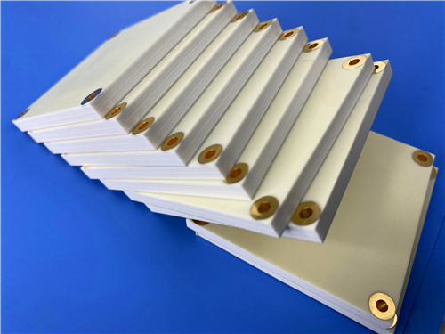
13.Standard Thicknesses, Panel Sizes & Claddings
Available Copper Foil Options
| Parameter | Specification |
|---|
| Copper foil type | ED copper |
| Copper foil thickness | 0.018 mm, 0.035 mm |
Standard Panel Sizes
| Panel Size | Tolerance |
|---|
| 150 × 150 mm | -2 mm |
| 160 × 160 mm | -2 mm |
| 200 × 200 mm | -2 mm |
| 170 × 240 mm | -2 mm |
Available Thicknesses and Tolerances
Note: The following thicknesses can be either total thickness including copper or dielectric thickness. Please specify when ordering whether you require "total thickness including copper" or "dielectric thickness".
Electrodeposited Copper Foil:
| Thickness (mm) | Tolerance (mm) |
|---|
| 0.5 | ±0.04 |
| 0.8 | ±0.05 |
| 1.0 | ±0.05 |
| 1.2 | ±0.05 |
| 1.5 | ±0.06 |
| 2.0 | ±0.075 |
| 3.0 | ±0.1 |
| 4.0 | ±0.1 |
| 5.0 | ±0.12 |
| 6.0 | ±0.12 |
| 7.0 | ±0.15 |
| 8.0 | ±0.18 |
| 10.0 | ±0.2 |
| 12.0 | ±0.3 |
|
|
.png)