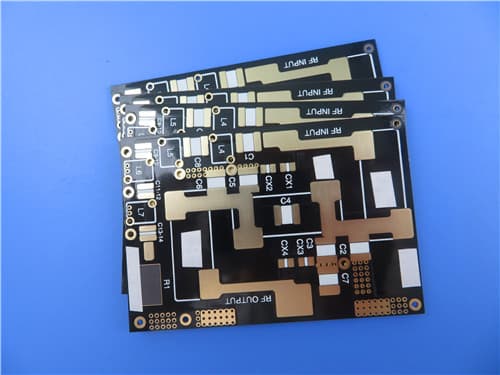
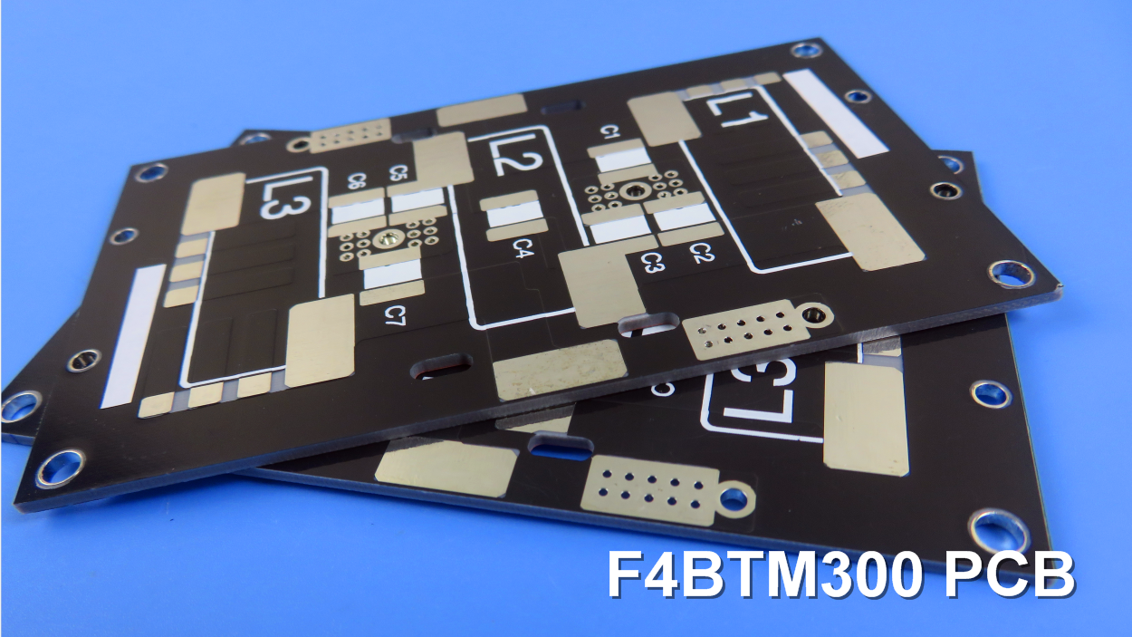
F4BTM350 2-Layer 3.1mm Thick PCB for High-Frequency RF & Microwave Applications1.Introduction of F4BTM350 Wangling's F4BTM350 laminates are engineered through a scientific formulation of fiberglass cloth, nano-ceramic fillers, and polytetrafluoroethylene resin, followed by stringent pressing processes. This series builds upon the F4BM dielectric layer by incorporating high-dielectric, low-loss nano-ceramic materials. The result is a laminate with a higher dielectric constant, improved heat resistance, a lower thermal expansion coefficient, higher insulation resistance, and enhanced thermal conductivity—all while maintaining excellent low-loss characteristics. F4BTM350 and F4BTME350 share the same dielectric layer but differ in copper foil type: F4BTM uses ED copper foil and is suitable for applications without PIM (Passive Intermodulation) requirements, while F4BTME uses reverse-treated (RTF) copper foil, offering superior PIM performance, more precise line control, and reduced conductor loss. 2.Key Features Dielectric constant (Dk) of 3.5 ±0.07 at 10GHz 3.Benefits of Using F4BTM350 in PCB Design Excellent high-frequency performance with stable Dk and low loss
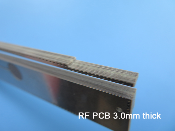
4.PCB Construction Details
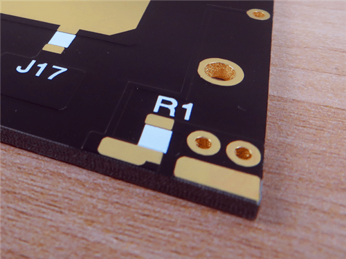
5.PCB Stackup (2-Layer Rigid Structure) Copper layer 1: 35µm 6.PCB Statistics: Components: 58 7.Typical Applications Microwave, RF, and radar systems 8.Quality Assurance Artwork Format: Gerber RS-274-X |
Get a Quick Quote
Fill in the form below and our engineers will reply within 24 hours with technical specifications and pricing for F4BTM350 2-Layer 3.1mm Thick PCB.

.jpg)