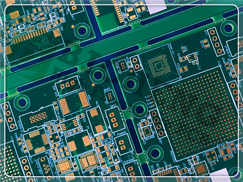
High-Performance Hybrid PCB: RO4003C and S1000-2M 6-Layer Construction
1.Introduction of RO4003C
RO4003C materials combine the electrical performance of PTFE with the manufacturability of epoxy/glass, offering excellent dielectric control and low loss.
2.Features
RO4003C:
Dielectric Constant: DK 3.38 +/-0.05 at 10GHz
Dissipation Factor: 0.0027 at 10GHz
Thermal Conductivity: 0.71 W/m/°K
Low moisture absorption: 0.06%
Ideal for multi-layer board constructions
S1000-2M
Lower Z-Axis CTE for improved reliability
Excellent thermal resistance and mechanical processability
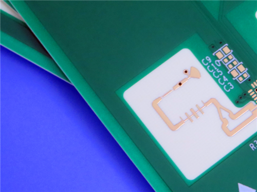
3. PCB Construction Details
| Specification | Details |
|---|
| Base Material | RO4003C + S1000-2M |
| Layer Count | 6 layers |
| Board Dimensions | 356mm x 373mm, 3 Types, 3PCS, +/- 0.15mm |
| Minimum Trace/Space | 4/4 mils |
| Minimum Hole Size | 0.35mm |
| Blind Vias | No |
| Finished Board Thickness | 2.0mm |
| Finished Cu Weight | 1oz (1.4 mils) inner/outer layers |
| Via Plating Thickness | 20 µm |
| Surface Finish | Hot Air Soldering Level (HASL) |
| Top Silkscreen | White |
| Bottom Silkscreen | No |
| Top Solder Mask | Blue |
| Bottom Solder Mask | No |
| Electrical Test | 100% Electrical Test Used Prior to Shipment |
4.PCB Stackup: 6-layer rigid PCB
Copper Layer 1: 35 µm
RO4003C: 0.508 mm (20 mil)
Copper Layer 2: 35 µm
Prepreg: 1080 X2 RC63% 0.127mm (5 mil)
Copper Layer 3: 35 µm
S1000-2M: 0.508 mm (20 mil)
Copper Layer 4: 35 µm
Prepreg: 1080 X2 RC63% 0.127mm (5 mil)
Copper Layer 5: 35 µm
S1000-2M: 0.508 mm (20 mil)
Copper Layer 6: 35 µm
5.PCB Statistics
Components: 122
Total Pads: 447
Thru Hole Pads: 229
Top SMT Pads: 218
Bottom SMT Pads: 0
Vias: 138
Nets: 8
6. Artwork Specifications and Standards
Type of Artwork Supplied: Gerber RS-274-X
Accepted Standard: IPC-Class-2
Availability: Worldwide
7. Typical Applications
Commercial Airline Broadband Antennas
Microstrip and Stripline Circuits
Millimeter Wave Applications
Radar Systems
Guidance Systems
Point to Point Digital Radio Antennas
|
.jpg)
.jpg)
