| |
Rogers TMM3 2-Layer 100mil EPIG High Frequency PCB for Microwave & RF Applications
1. Introduction to TMM3 High Frequency PCB
Rogers TMM 3 thermoset microwave material is a ceramic thermoset polymer composite designed for high plated thru-hole reliability strip-line and micro-strip applications.
TMM 3 laminates combine many of the benefits of both ceramic and traditional PTFE microwave circuit laminates without requiring the specialized production techniques common to those materials. TMM laminates are based on thermoset resins, making them reliable for wire-bonding without pad lifting or substrate deformation.
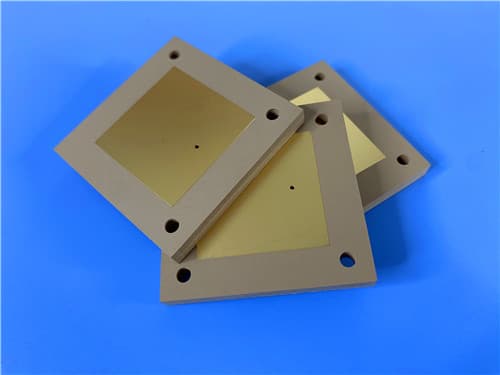
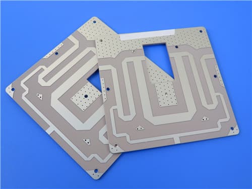
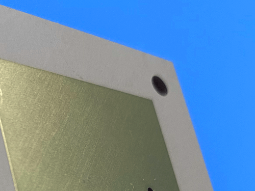
This 2-layer rigid PCB is constructed entirely with TMM3 as the core material at 100mil (2.54mm) thickness, with EPIG (nickel-free palladium gold) surface finish and 1oz copper on both sides. Its DK of 3.27 offers excellent high-frequency performance, making it ideal for demanding applications such as chip testers, dielectric polarizers, filters, GPS antennas, patch antennas, power amplifiers, and satellite communication systems.
2. Key Features
Dielectric Constant (DK): 3.27 ± 0.032 at 10GHz Dielectric Constant (Design): 3.45 (8 GHz - 40 GHz) Dissipation Factor (Df): 0.0020 at 10GHz Thermal Coefficient of DK (TCDK): 37 ppm/°K (-55°C to +125°C) CTE matched to copper: X-axis 15 ppm/K, Y-axis 15 ppm/K, Z-axis 23 ppm/K (0°C to 140°C) High Thermal Conductivity: 0.70 W/(M·K) — approximately twice that of traditional PTFE/ceramic laminates EPIG (Electroless Palladium Immersion Gold) – Nickel-free finish No solder mask, no silkscreen Board dimensions: 48.6mm x 50.04mm Finished board thickness: 2.54mm (100mil) Lead-Free Process Compatible
3. Benefits
Stable DK (3.27±0.032) — Consistent impedance control for high-frequency designs Low Df (0.0020 @ 10GHz) — Excellent high-frequency performance with minimal signal loss CTE Matched to Copper (15/15/23 ppm/K) — High reliability plated through holes, dimensional stability High Thermal Conductivity (0.70 W/m/K) — Approximately twice that of traditional PTFE/ceramic laminates Thermoset Resin — No softening when heated, reliable wire-bonding without pad lifting or substrate deformation Excellent Mechanical Properties — Resist creep and cold flow Chemical Resistance — Resistant to etchants and solvents used in PCB production No Sodium Napthanate Treatment Required — Simplified electroless plating process EPIG Nickel-Free Finish — Excellent solderability, wire bondability, and corrosion resistance without nickel concerns
4. PCB Construction Details
| Item | Specification |
|---|
| Base material | Rogers TMM3 (Ceramic Thermoset Polymer Composite) |
| Layer count | 2-layer rigid PCB |
| Board dimensions | 48.6mm x 50.04mm = 1 PCS |
| Minimum Hole Size | 2.5mm |
| Blind vias | No |
| Finished board thickness | 2.54mm (100mil) |
| Finished Cu weight | 1 oz (35 μm / 1.4 mils) all layers |
| Via plating thickness | 20 μm |
| Surface finish | EPIG (Electroless Palladium Immersion Gold – Nickel-Free) |
| Top Solder Mask | No |
| Bottom Solder Mask | No |
| Top Silkscreen | No |
| Bottom Silkscreen | No |
| Quality standard | IPC-Class-2 |
| 100% Electrical test | Used prior to shipment |
5. PCB Stackup (2-Layer Rigid Structure)
Layer 1 (Top Copper) – 35 μm (1 oz)
Rogers TMM3 Substrate – 2.54 mm (100mil)
Layer 2 (Bottom Copper) – 35 μm (1 oz)
6. PCB Statistics
Components: 1
Total Pads: 1
Thru Hole Pads: 1
Top SMT Pads: 1
Bottom SMT Pads: 0
Vias: 1
Nets: 2
7. Rogers TMM3 Material – Product Introduction
Rogers TMM 3 thermoset microwave material is a ceramic thermoset polymer composite designed for high plated thru-hole reliability strip-line and micro-strip applications.
TMM 3 laminates combine many of the benefits of both ceramic and traditional PTFE microwave circuit laminates without requiring the specialized production techniques common to those materials. TMM laminates are based on thermoset resins, making them reliable for wire-bonding without pad lifting or substrate deformation.
TMM laminates have an exceptionally low thermal coefficient of dielectric constant, typically less than 30 ppm/°C. The material's isotropic coefficients of thermal expansion, very closely matched to copper, allow for production of high reliability plated through holes, and low etch shrinkage values. Furthermore, the thermal conductivity of TMM laminates is approximately twice that of traditional PTFE/ceramic laminates, facilitating heat removal.
TMM laminates are based on thermoset resins, and do not soften when heated. As a result, wire bonding of component leads to circuit traces can be performed without concerns of pad lifting or substrate deformation.
TMM laminates combine many of the desirable features of ceramic substrates with the ease of soft substrate processing techniques. TMM laminates are available clad with 1/2 oz/ft² to 2 oz/ft² electrodeposited copper foil, or bonded directly to brass or aluminum plates. Substrate thicknesses of 0.015" to 0.500" are available. The base substrate is resistant to etchants and solvents used in printed circuit production. Consequently, all common PWB processes can be used to produce TMM thermoset microwave materials.

8. Features and Benefits Summary
| Feature | Benefit |
|---|
| DK 3.27 ± 0.032 @ 10GHz | Stable dielectric constant for consistent impedance control |
| Df 0.0020 @ 10GHz | Low loss for high-frequency RF and microwave designs |
| TCDK: 37 ppm/°K | Stable electrical performance over temperature |
| CTE: 15/15/23 ppm/K matched to copper | High reliability plated through holes, dimensional stability |
| Thermal conductivity 0.70 W/m/K | Efficient heat removal, ~2x that of traditional PTFE/ceramic laminates |
| Thermoset resin | No softening when heated, reliable wirebonding |
| No sodium napthanate treatment required | Simplified electroless plating process |
| Resistant to process chemicals | Reduces damage during fabrication and assembly |
| EPIG nickel-free finish | Excellent solderability, wire bondability, corrosion resistance |
9. TMM3 Typical Properties (Data Sheet)
| Property | Typical Value | Condition | Unit | Test Method |
|---|
| Electrical Properties |
| Dielectric Constant (Process) | 3.27 ± 0.032 | 10 GHz | — | IPC-TM-650 2.5.5.5 |
| Dielectric Constant (Design) | 3.45 | 8 GHz - 40 GHz | — | Differential Phase Length Method |
| Dissipation Factor (Process) | 0.0020 | 10 GHz | — | IPC-TM-650 2.5.5.5 |
| Thermal Coefficient of DK | +37 | -55°C to +125°C | ppm/°K | IPC-TM-650 2.5.5.5 |
| Insulation Resistance | >2000 | C/96/60/95 | GΩ | ASTM D257 |
| Volume Resistivity | 3×10⁹ | — | MΩ·cm | ASTM D257 |
| Surface Resistivity | >9×10⁹ | — | MΩ | ASTM D257 |
| Electrical Strength | 441 | Z direction | V/mil | IPC-TM-650 2.5.6.2 |
| Thermal Properties |
| Decomposition Temperature (Td) | 425 | — | °C | ASTM D3850 |
| CTE (X-axis) | 15 | 0°C to 140°C | ppm/K | ASTM E 831 / IPC-TM-650 2.4.41 |
| CTE (Y-axis) | 15 | 0°C to 140°C | ppm/K | ASTM E 831 / IPC-TM-650 2.4.41 |
| CTE (Z-axis) | 23 | 0°C to 140°C | ppm/K | ASTM E 831 / IPC-TM-650 2.4.41 |
| Thermal Conductivity | 0.70 | Z direction, 80°C | W/(M·K) | ASTM C518 |
| Specific Heat Capacity | 0.87 | — | J/g/K | Calculated |
| Mechanical & Physical Properties |
| Copper Peel Strength (after thermal stress) | 5.7 (1.0) | after solder float 1 oz EDC | lb/inch (N/mm) | IPC-TM-650 2.4.8 |
| Flexural Strength (MD/CMD) | 16.53 | — | kpsi | ASTM D790 |
| Flexural Modulus (MD/CMD) | 1.72 | — | Mpsi | ASTM D790 |
| Moisture Absorption (1.27mm / 0.050") | 0.06 | D/24/23 | % | ASTM D570 |
| Moisture Absorption (3.18mm / 0.125") | 0.12 | D/24/23 | % | ASTM D570 |
| Specific Gravity | 1.78 | — | — | ASTM D792 |
| Lead-Free Process Compatible | YES | — | — | — |
10. Primary Application Areas
RF and microwave circuitry Power amplifiers and combiners Filters and couplers Satellite communication systems Global Positioning Systems (GPS) Antennas Patch Antennas Dielectric polarizers and lenses Chip testers Stripline and microstrip applications requiring high plated thru-hole reliability
11. Quality Assurance
Type of artwork supplied: Gerber RS-274-X Accepted standard: IPC-Class-2 Availability: Worldwide 100% Electrical test prior to shipment No sodium napthanate treatment required prior to electroless plating
12. Standard Thickness, Panel Sizes & Claddings
| Parameter | Options |
|---|
| Standard Thicknesses | 0.015" (0.381mm), 0.025" (0.635mm), 0.030" (0.762mm), 0.050" (1.270mm), 0.060" (1.524mm), 0.075" (1.900mm), 0.100" (2.500mm), 0.125" (3.175mm), 0.150" (3.810mm), 0.200" (5.080mm), 0.250" (6.350mm), 0.500" (12.70mm) — all ±0.0015" |
| Standard Panel Sizes | 18"×12" (457mm×305mm), 18"×24" (457mm×610mm) — additional sizes available |
| Standard Claddings | Electrodeposited Copper: ½ oz (18μm), 1 oz (35μm); additional claddings including heavy metal and unclad available |
13. Data Source Notes
Prolonged exposure in an oxidative environment may cause changes to the dielectric properties of hydrocarbon based materials. The rate of change increases at higher temperatures and is highly dependent on the circuit design. Rogers recommends that the customer evaluate each material and design combination to determine fitness for use over the entire life of the end product. The design Dk is an average number from several different tested lots of material and on the most common thickness/s. For more detailed information, please contact Rogers Corporation. All test data are typical measurement values intended to assist customers in material selection. They do not constitute any express or implied warranty and do not guarantee performance in specific applications. Customers are responsible for verifying the suitability of Rogers materials for each application.
|
|

.png)