4 Layer PCB Blind Via FR4 Tg150 Immersion Gold Circuit Board
(Custom PCBs are tailored products; the images and specifications provided are for reference only.)
Product Overview
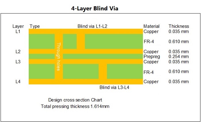
This multilayer PCB utilizes FR-4 substrate with Tg 150°C for mobile phone applications, featuring advanced blind via technology. The 1.6mm thick board combines white silkscreen (Taiyo) on green solder mask (Taiyo) with immersion gold finish for superior pad protection. Manufactured using ITEQ materials per IPC 6012 Class 2 standards, it includes blind vias connecting top-to-inner layer 1 and inner layer 3-to-bottom configurations. Shipped in batches of 25 boards with no minimum order quantity.
Key Features
Middle Tg FR-4 material delivers low Z-CTE and exceptional through-hole reliability while immersion gold finish ensures high solderability with minimal contamination. Our production capabilities include a 16,000㎡ facility handling 8,000+ PCB variants monthly with >98% on-time delivery rate. The multilayer design optimizes component connectivity in compact layouts.
Advanced PCB Via Technology:
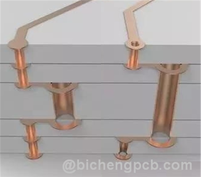
Blind/buried vias (GTL-L2, L3-L8, L3-GBL) and resin-filled microvias (≤0.4mm) for reliability.
Technical Specifications
Base Material: FR-4 Tg150°C (ITEQ)
Layer Count: 4 layers
Board Thickness: 1.6mm
Surface Finish: Immersion Gold
Solder Mask: Green (Taiyo)
Silkscreen: White (Taiyo)
Via Technology: Blind vias (top-L1/L3-bottom)
Certification: IPC 6012 Class 2
Applications
Industrial computing systems
GPS tracking devices
POS terminal hardware
Embedded control systems
Data acquisition modules
Microcontroller interfaces
Computer/notebook components
Parameter and data sheet
| PCB SIZE | 119 x 80mm=1PCS |
| BOARD TYPE | Multilayer PCB |
| Number of Layers | 4 layers |
| Surface Mount Components | YES |
| Through Hole Components | YES |
| LAYER STACKUP | copper ------- 18um(0.5oz)+plate TOP layer |
| Core FR-4 0.61mm | |
| copper ------- 35um(1oz) MidLayer 1 | |
| Prepreg 0.254mm | |
| copper ------- 35um(1oz) MidLayer 2 | |
| Core FR-4 0.61mm | |
| copper ------- 18um(0.5oz)+plate BOT layer | |
| TECHNOLOGY | |
| Minimum Trace and Space: | 4 mil / 4 mil |
| Minimum / Maximum Holes: | 0.3 mm /3.5 mm |
| Number of Different Holes: | 9 |
| Number of Drill Holes: | 415 |
| Number of Milled Slots: | 0 |
| Number of Internal Cutouts: | 0 |
| Impedance Control: | no |
| Number of Gold finger: | 0 |
| BOARD MATERIAL | |
| Glass Epoxy: | FR-4 Tg150℃, er<5.4.IT-158, ITEQ |
| Final foil external: | 1oz |
| Final foil internal: | 1oz |
| Final height of PCB: | 1.6mm ±0.16 |
| PLATING AND COATING | |
| Surface Finish | Immersion Gold |
| Solder Mask Apply To: | TOP and Bottom, 12micron Minimum |
| Solder Mask Color: | Green, PSR-2000 GT600D, Taiyo Supplied. |
| Solder Mask Type: | LPSM |
| CONTOUR/CUTTING | Routing, stamp holes. |
| MARKING | |
| Side of Component Legend | TOP and Bottom. |
| Colour of Component Legend | White, S-380W, Taiyo Supplied. |
| Manufacturer Name or Logo: | Marked on the board in a conductor and leged FREE AREA |
| VIA | Plated through hole(PTH), minimum size 0.3mm. Blind Via Top to Inner layer 1, Bottom to Inner layer 2 |
| FLAMIBILITY RATING | UL 94-V0 Approval MIN. |
| DIMENSION TOLERANCE | |
| Outline dimension: | 0.0059" |
| Board plating: | 0.0029" |
| Drill tolerance: | 0.002" |
| TEST | 100% Electrical Test prior shipment |
| TYPE OF ARTWORK TO BE SUPPLIED | email file, Gerber RS-274-X, PCBDOC etc |
| SERVICE AREA | Worldwide, Globally. |
.jpg)
Composition of Holes
1. Via Types
1.1 Blind Vias
Connect surface layers to adjacent inner layers
Depth controlled within aspect ratio limits
Enable high-density interconnects
1.2 Buried Vias
Connect inner layers only
Fabricated during pre-lamination
Maintain surface layer integrity
1.3 Through Vias
Penetrate entire board thickness
Most cost-effective solution
Default via type unless specified
2. Via Structure
Drill Hole: Conducts electrical signals
Pad Area: Provides mechanical support
3. Design Considerations
Smaller vias maximize routing space
Must maintain manufacturable aspect ratios
Critical for high-speed/high-density designs
Balance size reduction with reliability
This optimized via technology enables compact PCB layouts while ensuring signal integrity and manufacturing feasibility. Our engineering team can recommend the optimal via configuration for your specific application requirements.
