F4BM220 2-Layer 0.5mm ENIG PCB for Microwave and Radar Systems1.Introduction of F4BM220 Wangling's F4BM220 laminates are made by scientifically formulating and strictly pressing a combination of fiberglass cloth, polytetrafluoroethylene resin, and polytetrafluoroethylene film. Its electrical performance is improved compared to F4B220, mainly due to lower dielectric loss, increased insulation resistance, and improved stability. It can replace similar foreign products. F4BM220 and F4BME220 have the same dielectric layer but different copper foil combinations: F4BM220 is paired with ED copper foil, suitable for applications without PIM requirements; F4BME220 is paired with reverse-treated foil (RTF) copper foil, offering excellent PIM performance, more precise line control, and lower conductor loss. By adjusting the ratio between polytetrafluoroethylene and fiberglass cloth, F4BM220 and F4BME220 achieve precise control of the dielectric constant, providing low loss and enhanced dimensional stability. A higher dielectric constant corresponds to a higher proportion of fiberglass, resulting in better dimensional stability, lower thermal expansion coefficient, improved temperature drift, and a slight increase in dielectric loss. 2.Key Features Low Dielectric Constant: 2.2 ±0.04 at 10GHz
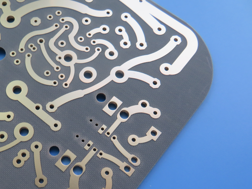
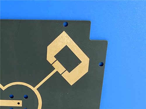
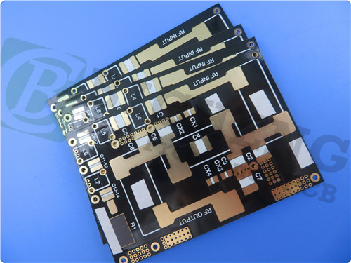
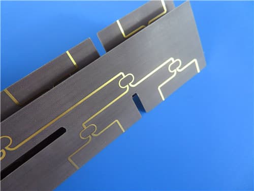
3.PCB Construction Details
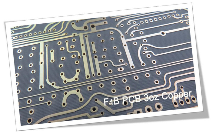
4.PCB Stackup (2-Layer Rigid Structure) Copper Layer 1 - 35 μm 5.PCB Statistics: Components: 5 6.Typical Applications Microwave, RF, and radar systems 7.Quality Assurance Artwork Format: Gerber RS-274-X |
Get a Quick Quote
Fill in the form below and our engineers will reply within 24 hours with technical specifications and pricing for F4BM220 2-Layer 0.5mm PCB.