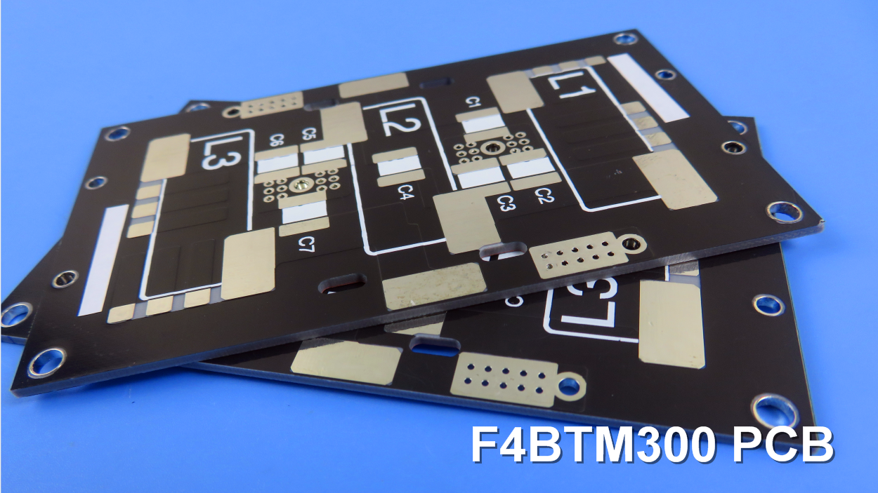
F4BTM300 2-Layer 10mil Ceramic-Filled PTFE PCB with ENIG Finish1.Introduction The F4BTM series laminates are manufactured through a meticulous process that involves the scientific formulation of glass fiber cloth, nano-ceramic fillers, and polytetrafluoroethylene (PTFE) resin. These substrates are built upon the F4BM dielectric layer and incorporate high dielectric constant and low loss nano-ceramics. This integration results in enhanced dielectric constant, superior heat resistance, reduced thermal expansion coefficient, increased insulation resistance, and improved thermal conductivity, all while maintaining low loss characteristics. Furthermore, F4BTM laminates are specifically paired with reverse-treated RTF copper foil, providing exceptional performance in terms of PIM, precise line control, and minimized conductor loss. 2.Key Features Dielectric constant (Dk) of 3 +/-0.06 at 10GHz 3.Benefits Enhanced dielectric constant and thermal performance with nano-ceramic fillers
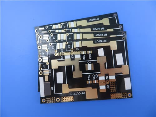
4.PCB Details
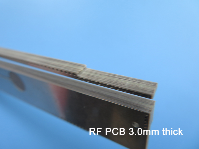
5.PCB Stackup (2-Layer Rigid Structure) Copper layer 1 – 35 μm 6.PCB Statistics Components: 29 7.Typical Applications Aerospace equipment, space and cabin equipment 8.Quality Assurance Artwork Format: Gerber RS-274-X |
Get a Quick Quote
Fill in the form below and our engineers will reply within 24 hours with technical specifications and pricing for F4BTM300 2-Layer 10mil PCB.

.jpg)