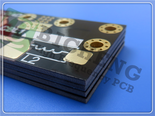
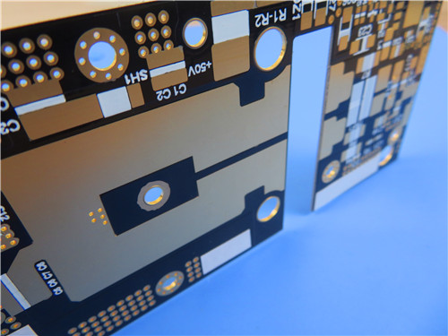
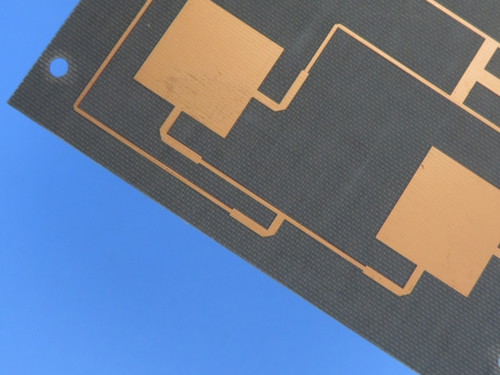
F4BTMS1000 PCB 2-Layer 6.35mm Thick High Thermal Conductivity for Aerospace and RF Feed Networks1.Overview of the F4BTMS Series The F4BTMS series represents an enhanced version of the F4BTM series, achieving significant advancements in material formulation and manufacturing processes. This upgraded material integrates a substantial amount of ceramics and is reinforced with ultra-thin, ultra-fine glass fiber cloth, leading to considerable improvements in performance and a wider range of dielectric constants. It is a highly reliable material ideal for aerospace applications and can effectively replace similar foreign products. By using a minimal quantity of ultra-thin glass fiber cloth along with a large volume of uniformly distributed specialized nano-ceramics mixed with polytetrafluoroethylene resin, the series mitigates the negative impacts of glass fiber on electromagnetic wave propagation. This results in reduced dielectric loss, improved dimensional stability, and lower X/Y/Z anisotropy. Furthermore, it enhances the usable frequency range, electrical strength, and thermal conductivity, while also exhibiting a low thermal expansion coefficient and stable dielectric temperature characteristics. A standard feature of the F4BTMS series is the RTF low roughness copper foil, which minimizes conductor loss and offers excellent peel strength. The material is compatible with both copper and aluminum substrates. 2. Features (F4BTMS1000) Dielectric constant (Dk): 10.2 at 10GHz
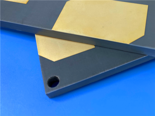
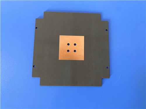
3. PCB Stackup Configuration: 2-layer rigid PCB 4. PCB Construction Details Board dimensions: 98mm x 98mm (1 piece), ± 0.15mm tolerance 5. PCB Statistics Components: 28 6.Type of Artwork Supplied Gerber RS-274-X 7. Quality Standard IPC-Class-2 8.Availability Worldwide 9. Typical Applications Aerospace equipment, space and cabin equipment |
Get a Quick Quote
Fill in the form below and our engineers will reply within 24 hours with technical specifications and pricing for F4BTMS1000 PCB 2-Layer 6.35mm Thick High Thermal Conductivity for Aerospace and RF Feed Networks.
.jpg)
