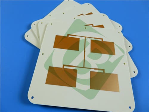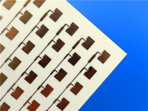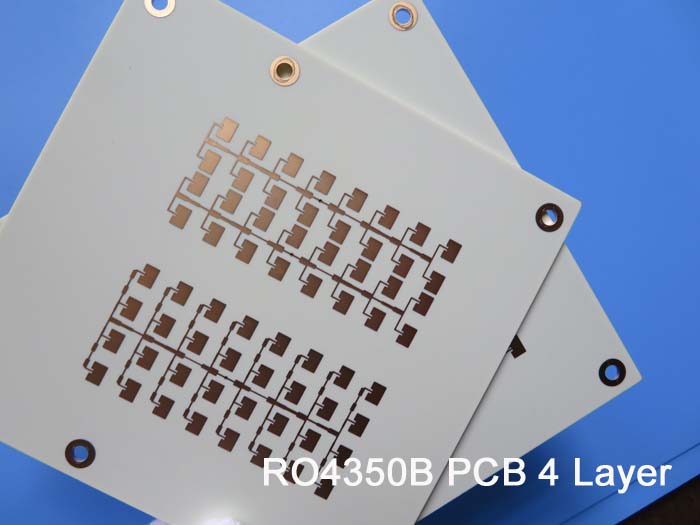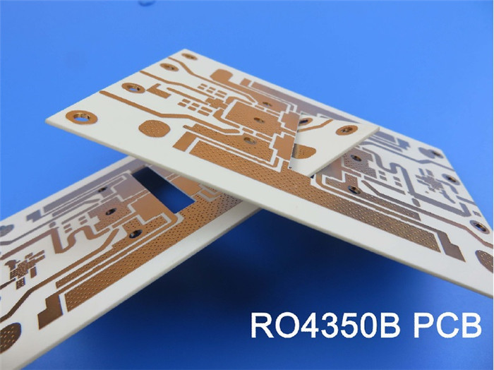
RO4350B PCB 2-Layer 13.3mil Low Loss Hydrocarbon/Ceramic Material for Multilayer Board Designs1.Introduction of RO4350B Rogers RO4350B materials consist of proprietary woven glass-reinforced hydrocarbon and ceramics, offering electrical performance comparable to PTFE/woven glass while retaining the manufacturability of epoxy/glass. These laminates provide precise control over dielectric constant (Dk) and low loss, utilizing standard epoxy/glass processing methods. Available at a significantly lower cost than traditional microwave laminates, RO4350B does not require special through-hole treatments or handling procedures typical of PTFE-based materials. Additionally, these materials are UL 94 V-0 rated, making them suitable for active devices and high-power RF applications. The thermal coefficient of expansion (CTE) of RO4350B materials presents several advantages for circuit designers. Its expansion coefficient is similar to that of copper, ensuring excellent dimensional stability, which is essential for mixed dielectric multi-layer board constructions. The low Z-axis CTE of RO4350B laminates guarantees reliable plated through-hole quality, even under severe thermal shock conditions. With a Tg exceeding 280°C (536°F), the expansion characteristics of RO4350B remain stable across the full range of circuit processing temperatures. 2. Features Dielectric Constant of DK 3.48 +/- 0.05 at 10 GHz/23°C
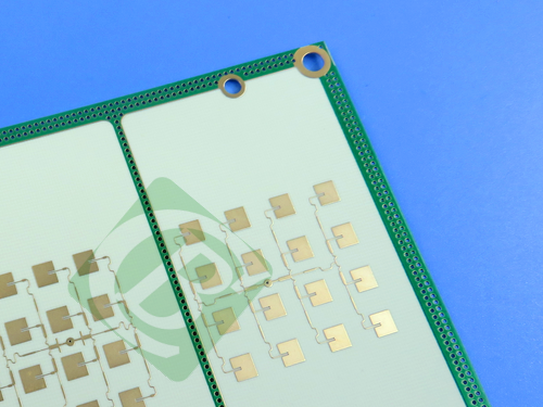
3. Benefits Suitable for multi-layer board (MLB) constructions 4.PCB Stackup: 2-layer rigid PCB 5.PCB Construction Detail Board dimensions: 40 mm x 40 mm = 1 PCS, +/- 0.15 mm 6.PCB Statistics 7.Type of Artwork Supplied: 8.Quality Standard: 9. Availability: 10. Some Typical Applications Cellular base station antennas and power amplifiers |
Get a Quick Quote
Fill in the form below and our engineers will reply within 24 hours with technical specifications and pricing for Rogers RO4350B PCB 2-Layer 13.3mil Low Loss Hydrocarbon/Ceramic Material for Multilayer Board Designs.