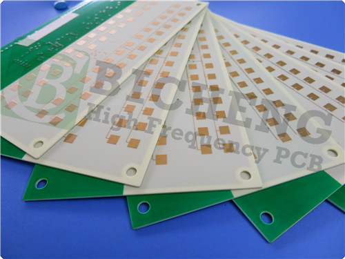
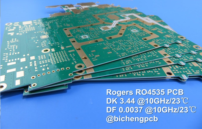
RO4535 PCB 2-Layer 20mil High-Frequency Laminates for Antenna and Mobile Infrastructure Applications1.Introduction of RO4535 RO4535 High Frequency Laminates are cost-effective performance materials developed by Rogers Corporation to address the specific needs of the antenna market. These laminates expand on the capabilities of the successful RO4000 series, offering a ceramic-filled, glass-reinforced hydrocarbon material that ensures a controlled dielectric constant, low loss performance, and excellent passive intermodulation response, making them ideal for mobile infrastructure microstrip antenna applications. RO4535 laminates are fully compatible with standard FR-4 and high-temperature lead-free solder processing. Unlike traditional PTFE-based laminates, they do not require special treatments for plated through-hole preparation. This product presents an affordable alternative to conventional PTFE antenna technologies, enabling designers to optimize both cost and performance for their antennas. Additionally, RO4535 laminates are available with Rogers' RoHS-compliant flame-retardant technology for applications that necessitate UL94 V-0 certification. 2.Feature Dielectric Constant of DK 3.44 +/-0.08 at 10 GHz/23°C
3. Benefits Exceptional passive intermodulation (PIM) performance with LoPro copper foil 4.PCB Stackup: 2-layer rigid PCB 5.PCB Construction Detail Board dimensions: 53 mm x 53 mm = 1 PCS, +/- 0.15 mm 6.PCB Statistics 7.Type of Artwork Supplied: 8.Quality Standard: 9. Availability: 10. Some Typical Applications Antennas for cellular infrastructure base stations |
Get a Quick Quote
Fill in the form below and our engineers will reply within 24 hours with technical specifications and pricing for Rogers RO4535 PCB 2-Layer 20mil High-Frequency Laminates for Antenna and Mobile Infrastructure Applications.
.jpg)
