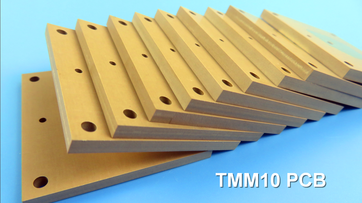
Rogers TMM13i 2-Layer 3.9mm OSP PCB for Chip Tester & Satellite Communication1.Introduction to TMM13i PCB The Rogers TMM13i isotropic thermoset microwave material is a ceramic thermoset polymer composite tailored for high reliability in plated thru-hole strip-line and micro-strip applications. It features an isotropic dielectric constant (Dk) and integrates the advantageous properties of both ceramic and PTFE substrates, while allowing for the convenience of soft substrate processing methods. This 2-layer rigid PCB is constructed entirely with TMM13i as the core material, providing excellent signal integrity, thermal stability, and high-dielectric-constant performance for demanding RF and microwave applications. 2.Key Features of TMM13i
3. Benefits of TMM13i PCB
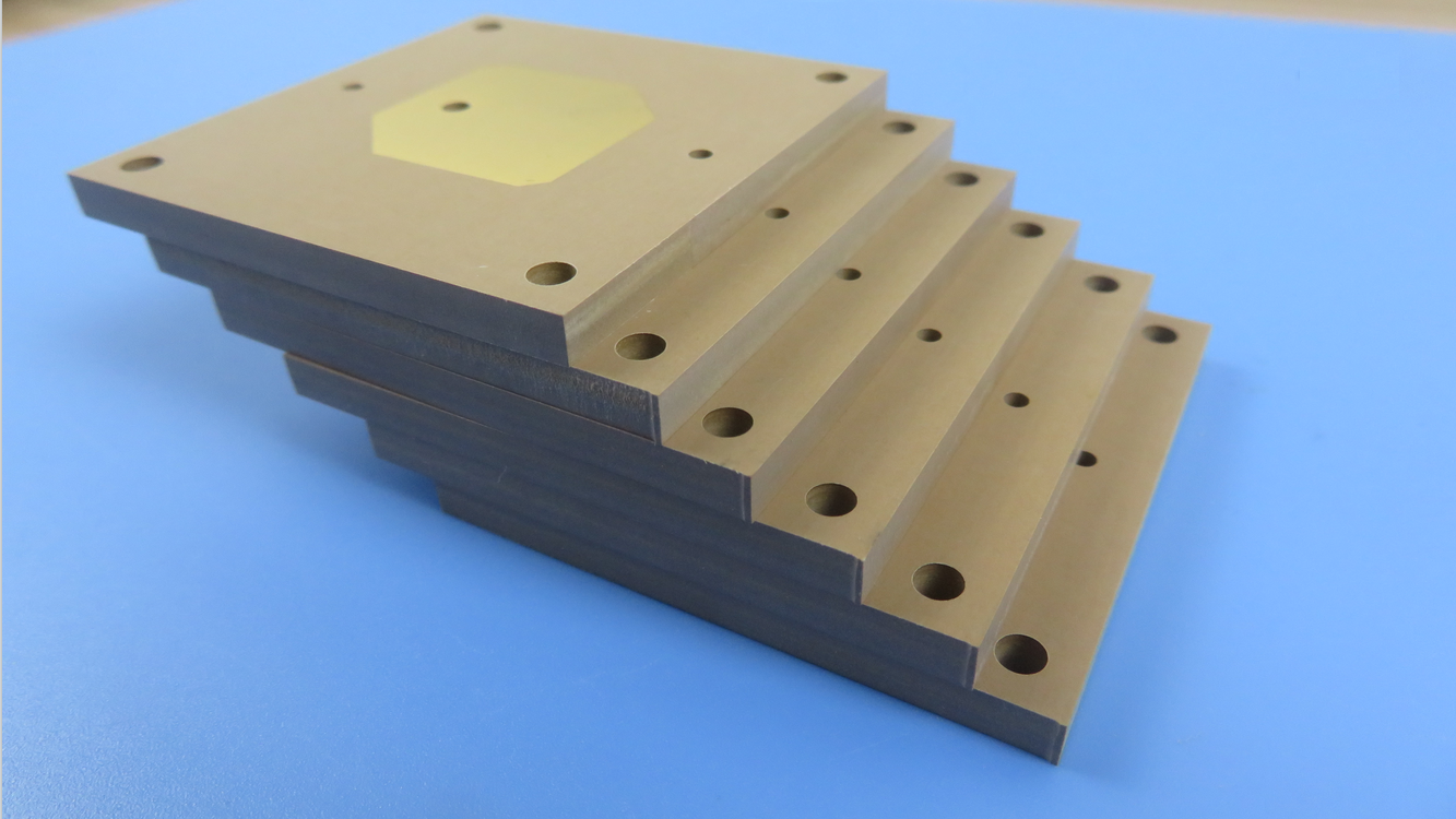
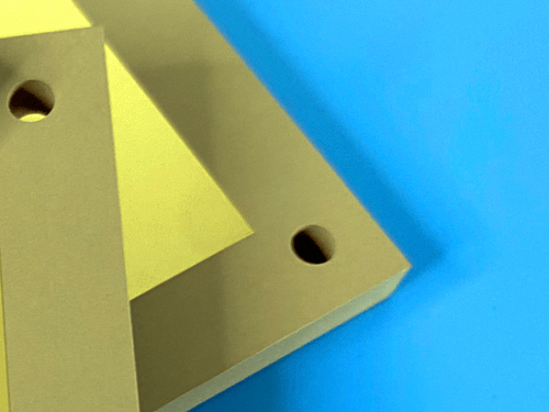
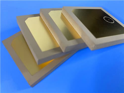
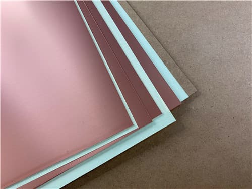
4.TMM13i PCB Construction Details
5.PCB Stackup (2-Layer Rigid Structure) Copper_layer_1 – 35 μm 6.PCB Statistics Components: 29 7.Primary Application Areas
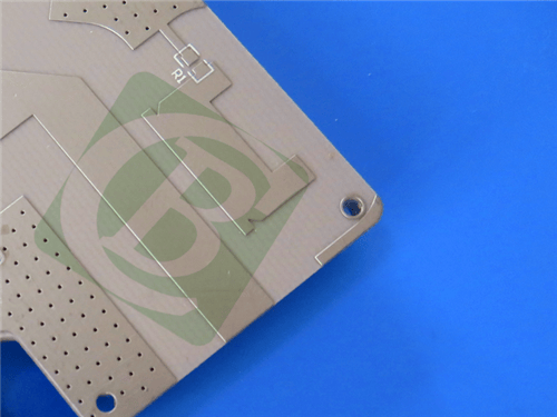
8.Quality Assurance Artwork supplied: Gerber RS-274-X
9.TMM® Thermoset Microwave Materials – TMM13i High Frequency Materials TMM® thermoset microwave materials are ceramic, hydrocarbon, thermoset polymer composites designed for high plated-thru-hole reliability stripline and microstrip applications. TMM laminates are available in a wide range of dielectric constants and claddings. The electrical and mechanical properties of TMM laminates combine many of the benefits of both ceramic and traditional PTFE microwave circuit laminates, without requiring the specialized production techniques common to these materials. TMM laminates do not require a sodium napthanate treatment prior to electroless plating. TMM laminates have an exceptionally low thermal coefficient of dielectric constant, typically less than 30 ppm/°C. The material's isotropic coefficients of thermal expansion, very closely matched to copper, allow for production of high reliability plated through holes, and low etch shrinkage values. Furthermore, the thermal conductivity of TMM laminates is approximately twice that of traditional PTFE/ceramic laminates, facilitating heat removal. TMM laminates are based on thermoset resins, and do not soften when heated. As a result, wire bonding of component leads to circuit traces can be performed without concerns of pad lifting or substrate deformation. TMM laminates combine many of the desirable features of ceramic substrates with the ease of soft substrate processing techniques. TMM laminates are available clad with 1/2 oz/ft² to 2 oz/ft² electrodeposited copper foil, or bonded directly to brass or aluminum plates. Substrate thicknesses of 0.015" to 0.500" are available. The base substrate is resistant to etchants and solvents used in printed circuit production. Consequently, all common PWB processes can be used to produce TMM thermoset microwave materials. The Rogers TMM13i isotropic thermoset microwave material is a ceramic thermoset polymer composite tailored for high reliability in plated thru-hole strip-line and micro-strip applications. It features an isotropic dielectric constant (Dk) and integrates the advantageous properties of both ceramic and PTFE substrates, while allowing for the convenience of soft substrate processing methods. 10.Features and Benefits Features
Benefits
11.TMM13i Data Sheet
12.Some Typical Applications
13.Standard Thicknesses, Panel Sizes & Claddings Standard Thicknesses
Standard Panel Sizes
Standard Claddings (Electrodeposited Copper Foil)
|
Get a Quick Quote
Fill in the form below and our engineers will reply within 24 hours with technical specifications and pricing for Rogers TMM13i 2-Layer 3.9mm OSP PCB.