Taconic TC350 + Isola FR408HR 8-Layer Hybrid PCB with Resin-Filled Vias, Edge Plating, and ENIG Finish
1. TC350 Material Introduction
TC350 is a ceramic-filled PTFE/woven fiberglass laminate developed by Taconic, specifically engineered for microwave printed circuit boards requiring enhanced thermal conductivity. The material combines the low-loss characteristics of PTFE with ceramic fillers to achieve improved heat dissipation while maintaining excellent high-frequency performance. TC350 features a dielectric constant of 3.50 and is available in various thicknesses with standard electrodeposited or reverse-treated copper foils. It is ideal for applications where both electrical performance and thermal management are critical.
2. TC350 Key Features and Benefits
Dk 3.50 (stable across frequency) ensures consistent impedance control
Df 0.0015 at 1 MHz, 0.0018 at 1.8 GHz, 0.0020 at 10 GHz provides low signal loss
Thermal conductivity 0.72 W/m·K enables superior heat dissipation
Td 520°C (initial), 567°C (5% weight loss) for excellent thermal stability
CTE X/Y: 7 ppm/°C matched to copper for dimensional stability
Z-axis CTE 23 ppm/°C with only 1.2% expansion from 50°C to 260°C
Volume resistivity 7.4 × 10⁶ MΩ·cm (C96/35/90) to 1.4 × 10⁸ MΩ·cm (E24/125)
Surface resistivity 3.2 × 10⁷ MΩ (C96/35/90) to 4.3 × 10⁸ MΩ (E24/125)
Copper peel strength 7-9 lbs/in (1.2-1.6 N/mm) after thermal stress
Moisture absorption only 0.05% maintains electrical stability
UL 94 V-0 rated for safety compliance
NASA low outgassing (TML 0.02%, CVCM 0.01%) for space applications
3. TC350 Data Sheet Summary
| Property |
Conditions |
Typical Value |
Unit |
Test Method |
| Dielectric Constant (Dk) |
@ 1 MHz |
3.50 |
- |
IPC TM-650 2.5.5.3 |
|
@ 1.8 GHz |
3.50 |
- |
Resonant Cavity |
|
@ 10 GHz |
3.50 |
- |
IPC TM-650 2.5.5.5 |
| Dissipation Factor (Df) |
@ 1 MHz |
0.0015 |
- |
IPC TM-650 2.5.5.3 |
|
@ 1.8 GHz |
0.0018 |
- |
Resonant Cavity |
|
@ 10 GHz |
0.0020 |
- |
IPC TM-650 2.5.5.5 |
| Thermal Coefficient of Dk |
-40°C to 150°C |
-9 |
ppm/°C |
IPC TM-650 2.5.5.5 |
| Volume Resistivity |
C96/35/90 |
7.4 × 10⁶ |
MΩ·cm |
IPC TM-650 2.5.17.1 |
|
E24/125 |
1.4 × 10⁸ |
MΩ·cm |
IPC TM-650 2.5.17.1 |
| Surface Resistivity |
C96/35/90 |
3.2 × 10⁷ |
MΩ |
IPC TM-650 2.5.17.1 |
|
E24/125 |
4.3 × 10⁸ |
MΩ |
IPC TM-650 2.5.17.1 |
| Electrical Strength |
- |
780 (31) |
V/mil (kV/mm) |
IPC TM-650 2.5.6.2 |
| Dielectric Breakdown |
- |
40 |
kV |
IPC TM-650 2.5.6 |
| Arc Resistance |
- |
>240 |
sec |
IPC TM-650 2.5.1 |
| Decomposition Temp (Td) |
Initial |
520 |
°C |
IPC TM-650 2.4.24.6 |
|
5% weight loss |
567 |
°C |
IPC TM-650 2.4.24.6 |
| Time to Delamination |
T260/T288/T300 |
>60 |
Minutes |
IPC TM-650 2.4.24.1 |
| CTE - X axis |
50°C to 150°C |
7 |
ppm/°C |
IPC TM-650 2.4.41 |
| CTE - Y axis |
50°C to 150°C |
7 |
ppm/°C |
IPC TM-650 2.4.41 |
| CTE - Z axis |
50°C to 150°C |
23 |
ppm/°C |
IPC TM-650 2.4.41 |
| Z-axis Expansion |
50°C to 260°C |
1.2 |
% |
IPC TM-650 2.4.24 |
| Thermal Conductivity |
- |
0.72 |
W/m·K |
ASTM D5470 |
| Specific Heat |
- |
0.90 |
J/g/K |
ASTM D5470 |
| Copper Peel Strength |
After Thermal Stress |
7 (1.2) |
lbs/in (N/mm) |
IPC TM-650 2.4.8 |
|
@ 150°C |
9 (1.6) |
lbs/in (N/mm) |
IPC TM-650 2.4.8.2 |
| Tensile Strength (MD/CMD) |
- |
11/8 (76/55) |
kpsi (MPa) |
IPC TM-650 2.4.18.3 |
| Flexural Strength (MD/CMD) |
- |
14/10 (97/69) |
kpsi (MPa) |
IPC TM-650 2.4.4 |
| Flammability |
UL 94 |
V-0 |
- |
UL 94 |
| Moisture Absorption |
- |
0.05 |
% |
IPC TM-650 2.6.2.1 |
| Density |
Method A |
2.3 |
g/cm³ |
ASTM D792 |
| NASA Outgassing - TML |
125°C, ≤10⁻⁶ torr |
0.02 |
% |
NASA SP-R-0022A |
| NASA Outgassing - CVCM |
125°C, ≤10⁻⁶ torr |
0.01 |
% |
NASA SP-R-0022A |
| NASA Outgassing - WVR |
125°C, ≤10⁻⁶ torr |
0.01 |
% |
NASA SP-R-0022A |
4. FR408HR Material Introduction
FR408HR is a high-performance FR-4 resin system from Isola Group, designed for multilayer PCB applications requiring maximum thermal performance and reliability. It features a high glass transition temperature (Tg) and is manufactured with Isola's patented high-performance multifunctional resin system, reinforced with electrical grade E-glass fabric. FR408HR delivers 30% improvement in Z-axis expansion and 25% more electrical bandwidth (lower loss) than competitive products, bridging the gap between thermal and electrical performance. The system is laser fluorescing and UV blocking for maximum compatibility with AOI systems, optical positioning, and photo-imageable solder mask imaging.
5. FR408HR Key Features and Benefits
Tg 190°C (DSC) ensures dimensional stability during lead-free processing
Td 360°C at 5% weight loss for excellent thermal decomposition resistance
T260 >60 min, T288 >30 min for superior delamination resistance
Z-axis CTE 55 ppm/°C pre-Tg, 230 ppm/°C post-Tg with total expansion 2.8%
X/Y-axis CTE 16 ppm/°C matched to copper for dimensional stability
Dk 3.68 at 2 GHz, 3.65 at 10 GHz for consistent impedance control
Df 0.0092 at 2 GHz, 0.0095 at 10 GHz for mid-loss performance
Thermal conductivity 0.4 W/m·K
Volume resistivity 4.4 × 10⁷ MΩ-cm (after moisture) to 9.4 × 10⁷ MΩ-cm (elevated temp)
Dielectric breakdown >50 kV and electric strength 70 kV/mm
CTI Class 2 (250-399V) for improved surface insulation reliability
Peel strength 1.14 N/mm (low profile) to 0.90 N/mm (standard profile)
Moisture absorption 0.061% maintains electrical properties in humid environments
UL 94 V-0 rated for safety compliance
Laser fluorescing and UV blocking for AOI compatibility
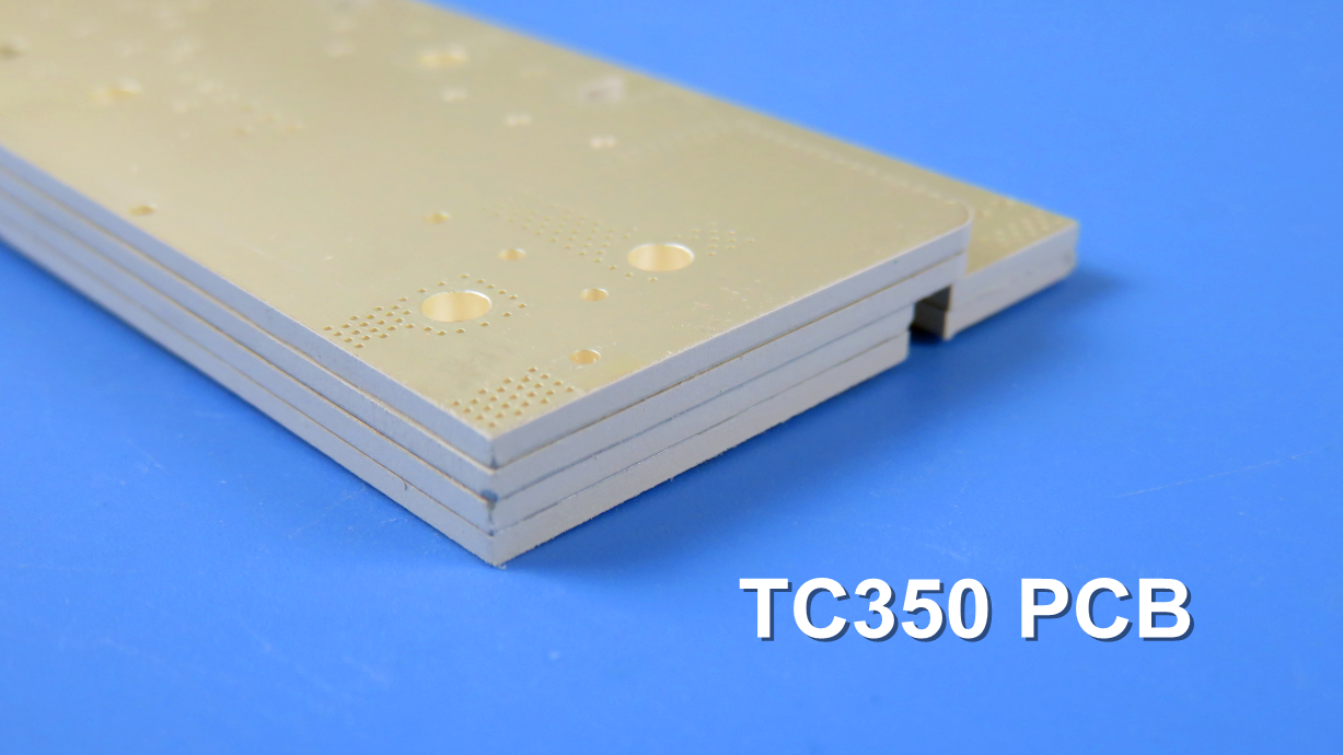
6. PCB Construction Details
| Item |
Specification |
| Product Type | 8-Layer Hybrid RF/Microwave PCB |
| High-Frequency Cores | Taconic TC350 (0.254mm × 2 sheets) |
| Mid-Loss Cores | Isola FR408HR (0.254mm × 2 sheets) |
| Prepreg | Rogers RO4450F |
| Layer Count | 8 Layers |
| Copper Thickness | 1oz (approx. 35μm) all layers |
| Finished Thickness | 2.0mm |
| Surface Finish | ENIG (Electroless Nickel Immersion Gold) |
| Solder Mask | Green |
| Silkscreen | White |
| Via Type | Blind vias |
| Via Process | 0.2mm vias, resin-filled and capped |
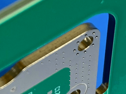
| Special Feature | Edge plating (metal wrap-around) |
| Dimensions | 99mm x 83mm = 1 PC |
| Design Standard | IPC-Class-2 |
| Artwork Format | Gerber RS-274-X |
| Availability | Worldwide |
7. PCB Stackup (8-Layer Rigid Structure)
L1 (Top): 1oz Copper
Core 1: TC350, 0.254mm
L2: 1oz Copper
Prepreg: RO4450F × 2 sheets, total 0.204mm
L3: 1oz Copper
Core 2: FR408HR, 0.254mm
L4: 1oz Copper
Prepreg: RO4450F × 2 sheets, total 0.204mm
L5: 1oz Copper
Core 3: FR408HR, 0.254mm
L6: 1oz Copper
Prepreg: RO4450F × 2 sheets, total 0.204mm
L7: 1oz Copper
Core 4: TC350, 0.254mm
L8 (Bottom): 1oz Copper
8. Primary Application Areas
RF and Microwave Systems: Base stations, wireless infrastructure
High-Speed Digital Designs: Servers, switches, routers
Radar Systems: Automotive radar, defense radar
Aerospace and Defense: Avionics, satellite communications
Test and Measurement Equipment: High-frequency analyzers
5G/6G Infrastructure: mmWave antennas, front-end modules
Broadband Communications: Microwave backhaul, satellite terminals
High-Reliability Computing: Data centers, high-performance computing
9. Quality Assurance
Artwork supplied: Gerber RS-274-X
Accepted standard: IPC-Class-2
Availability: Worldwide
10. What is Via Filled and Capped?
Via filling and capping is an advanced PCB manufacturing process where via holes are completely filled with non-conductive epoxy resin, then plated over with copper to create a flat, planar surface.
Process steps:
Drill via holes
Plate via barrels with copper
Fill vias with epoxy resin
Cure and planarize the resin
Plate copper cap over the filled via
Benefits:
Enables via-in-pad design for higher component density
Prevents solder wicking during assembly
Provides flat surface for component mounting
Improves thermal management
Enhances reliability by eliminating voids
Supports finer pitch components
11. What is Edge Plating and Why Use It?
Edge plating (also known as side plating or edge metallization) is a process where the perimeter edges of a PCB are plated with copper and finished with the board's surface finish. This creates a conductive path along the board edges.
Benefits:
EMI/RFI shielding: Creates continuous Faraday cage around the board
Enhanced grounding: Provides additional ground paths between layers
Thermal dissipation: Helps conduct heat away from board edges
Mechanical protection: Protects exposed substrate from moisture and damage
Improved solderability: Enables edge connections for board mounting
Reduced parasitics: Minimizes edge effects in high-frequency designs
|
.jpg)
.jpg)
