Home > Newly Shipped PCB > DiClad 870 2-Layer 93mil PCB – High-Frequency, Low-Loss, Immersion Gold Finish for RF Applications

DiClad 870 2-Layer 93mil High-Frequency Low-Loss PCB
PCB Material:Rogers DiClad 870 / 2.5mm finished thickness
MOQ:1PCS
Price:39.99-139 USD/PCS
Packaging:Vacuum / Anti-static Packaging
Delivery Period:8-16 working days
Payment Method:T/T, Paypal
 

DiClad 870 2-Layer 93mil PCB – High-Frequency, Low-Loss, Immersion Gold Finish for RF Applications


1.Introduction of DiClad 870

Rogers DiClad 870 laminates are woven fiberglass reinforced, PTFE-based composites designed for use as high-performance printed circuit board substrates. By utilizing fewer plies of woven fiberglass and a higher ratio of PTFE content, DiClad 870 offers a lower dielectric constant (Dk) and dissipation factor compared to other laminates in the DiClad series, making it ideal for high-frequency and low-loss applications.


2.Key Features

Dielectric Constant (Dk): 2.33 at 10 GHz and 1 MHz, 50% RH
Dissipation Factor: 0.0013 at 10 GHz, 0.0009 at 1 MHz, 50% RH
Thermal Coefficient of Dk (TcDK): -161 ppm/°C from -10°C to 140°C at 10 GHz
Arc Resistance: >180 seconds
Moisture Absorption: 0.02%
CTE: X-axis: 17 ppm/°C, Y-axis: 29 ppm/°C, Z-axis: 217 ppm/°C
Copper Peel Strength: 14 lbs/in, 10s @288°C
Flammability Rating: UL 94-V0


3.Benefits

Lowest moisture absorption among PTFE-based composites
Stable dielectric constant over a wide frequency range
Low Dk supports wider line widths for reduced insertion loss


DiClad 870 PCB


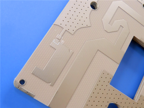
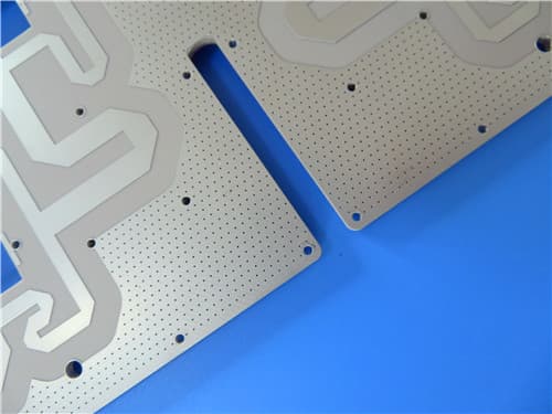
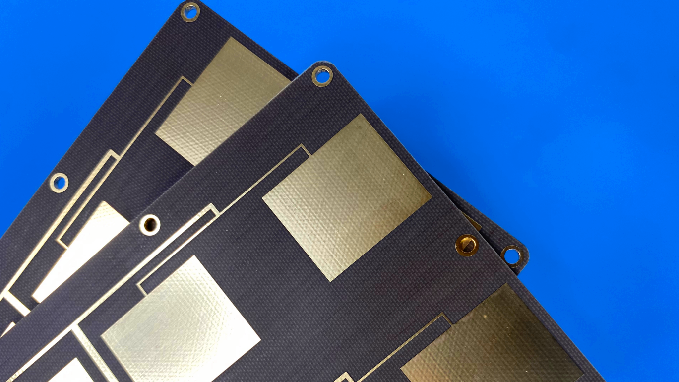
4.PCB Construction Details

ParameterSpecification
Base MaterialDiClad 870
Layer Count2-layer
Board Dimensions83mm × 35mm (±0.15mm)
Minimum Trace/Space5/9 mils
Minimum Hole Size0.3mm
Blind ViasNo
Finished Board Thickness2.5mm
Finished Cu Weight1oz (1.4 mils) outer layers
Via Plating Thickness20 μm
Surface FinishImmersion Gold
Top SilkscreenNo
Bottom SilkscreenNo
Top Solder MaskNo
Bottom Solder MaskNo
Electrical Test100% tested prior to shipment

5.PCB Stackup (2-Layer Rigid Structure)

Copper_layer_1 - 35 μm
DiClad 870 - 2.362 mm (93mil)
Copper_layer_2 - 35 μm


6.PCB Statistics:

Components: 11
Total Pads: 40
Thru Hole Pads: 24
Top SMT Pads: 16
Bottom SMT Pads: 0
Vias: 19
Nets: 2


7.Typical Applications

Radar Feed Networks
Commercial Phased Array Networks
Low-Loss Base Station Antennas
Guidance Systems
Digital Radio Antennas
Filters, Couplers, LNAs


8.Quality Assurance

IPC-Class 2 compliant
100% electrical tested
Global availability
Gerber RS-274X support


Get a Quick Quote

Fill in the form below and our engineers will reply within 24 hours with technical specifications and pricing for DiClad 870 2-Layer 93mil Low-Loss High-Frequency PCB with Immersion Gold Finish.

No file chosen

Max 10MB/file: .zip, .pdf, .jpg, .png, .txt (multiple)

Your information is safe. We'll respond within 24 hours.

Previous F4BTMS220 2-Layer 5mil PCB – Ultra-Thin High-Frequency Board with Immersion Gold for Aerospace and RF Applications

Next CuClad 233 2-Layer 20mil PCB – High-Frequency RF Board with Immersion Gold Finish