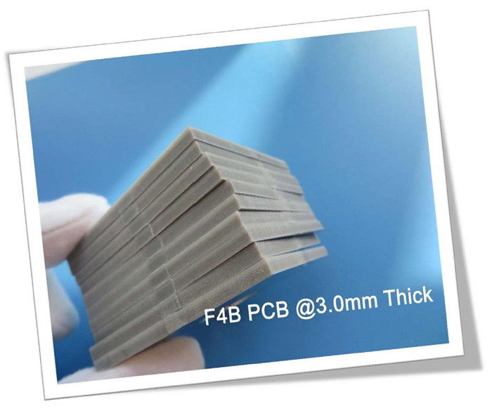
F4BM220 High-Performance 2-Layer PCB for Microwave and RF Applications1.INTRODUCTION TO F4BM220 Wangling's F4BM220 laminates are developed through a precise formulation and pressing of fiberglass cloth, polytetrafluoroethylene (PTFE) resin, and PTFE film. Compared to F4B220, it offers improved electrical performance due to lower dielectric loss, higher insulation resistance, and enhanced stability, making it a suitable alternative to similar foreign products. The F4BM220 and F4BME220 share the same dielectric layer but use different copper foil combinations: F4BM220 utilizes ED copper foil for applications without PIM requirements, while F4BME220 employs reverse-treated foil (RTF) for excellent PIM performance and reduced conductor loss. By adjusting the ratio of PTFE to fiberglass cloth, both F4BM220 and F4BME220 achieve precise control over the dielectric constant, resulting in low loss and enhanced dimensional stability. 2.FEATURES OF F4BM220 Dielectric Constant (Dk): 2.2 ± 0.04 at 10GHz
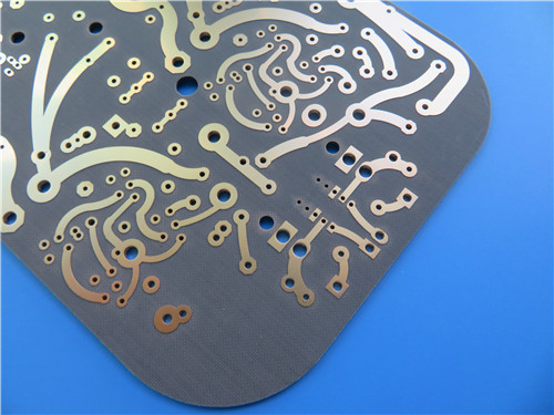
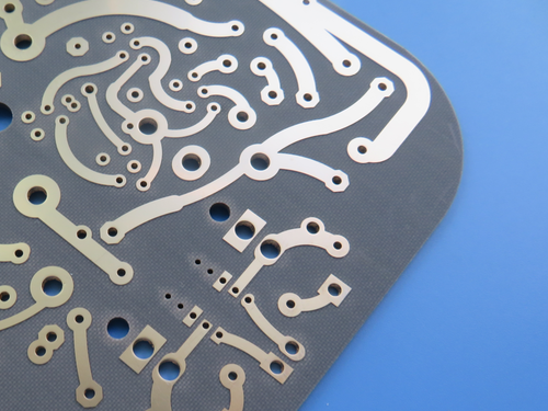
3.PCB CONSTRUCTION DETAILS
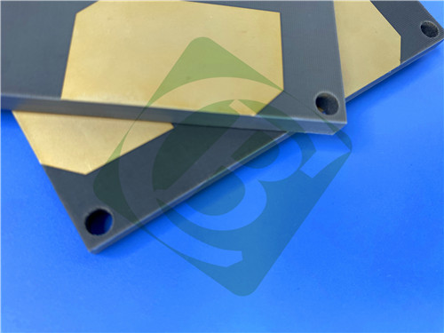
4. PCB STACKUP
5. PCB STATISTICS Components: 43 7.TYPICAL APPLICATIONS Microwave, RF, and radar systems |
Get a Quick Quote
Fill in the form below and our engineers will reply within 24 hours with technical specifications and pricing for F4BM220 High-Performance 2-Layer PCB for Microwave and RF Applications.