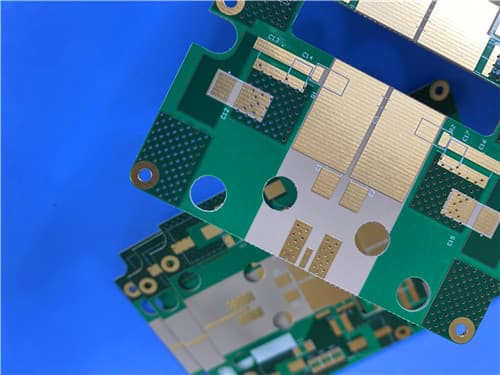
Isola I-Tera MT40 6-Layer PCB with Resin-Filled Vias, Edge Plating, and ENIG Finish
1. I-Tera MT40 Material Introduction
I-Tera MT40 is a high-performance laminate material developed by Isola Group, specifically designed for high-speed digital and RF/microwave printed circuit applications. It features a dielectric constant (Dk) that remains stable between -55°C and +125°C up to W-band frequencies, ensuring consistent electrical performance across a wide temperature range. With a low dissipation factor (Df) of 0.0031, I-Tera MT40 offers a cost-effective alternative to PTFE and other commercial microwave and high-speed digital laminate materials.
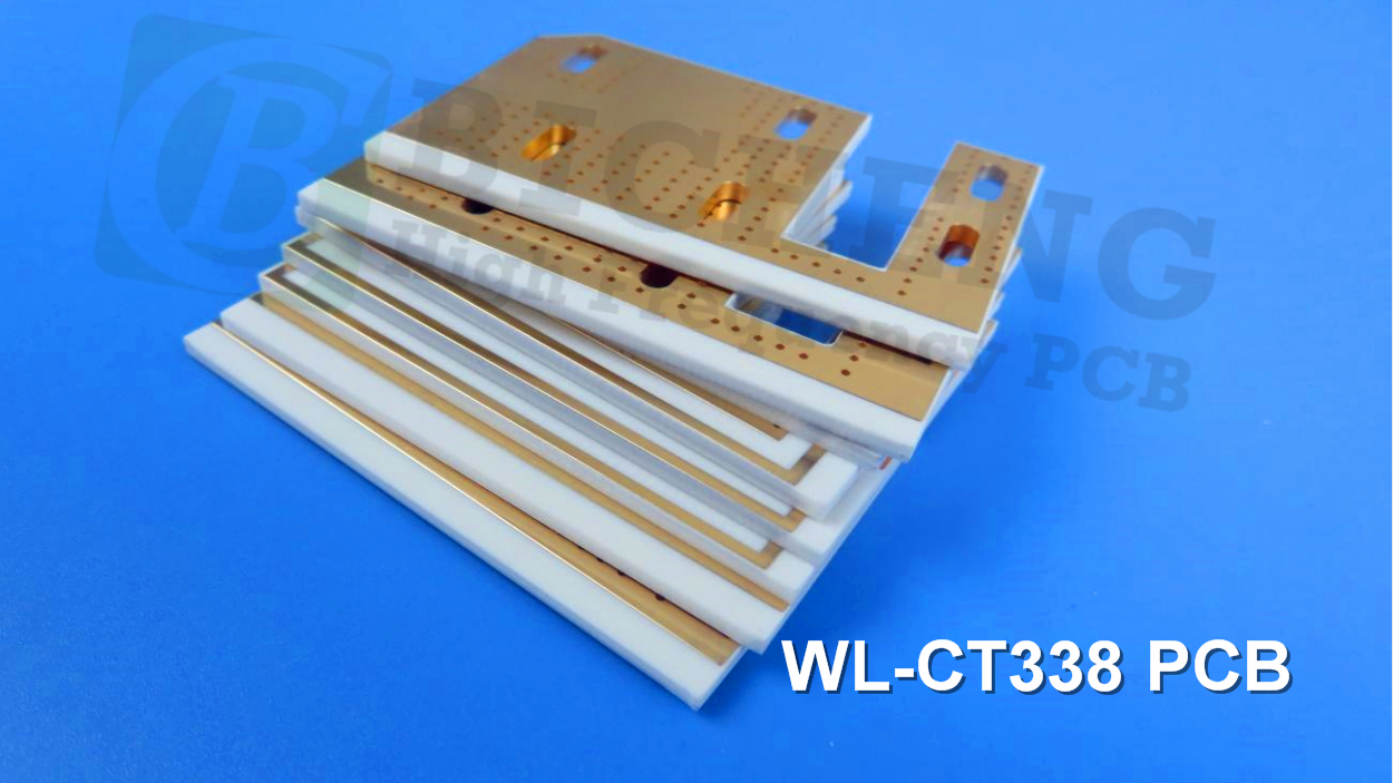
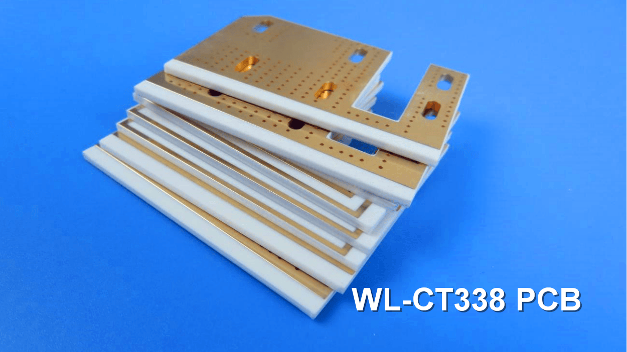
I-Tera MT40 is available in both laminate and prepreg form in typical thicknesses and standard panel sizes, providing a complete materials solution for high-speed digital multilayer, hybrid, RF/microwave, multilayer, and double-sided printed circuit designs. Importantly, I-Tera MT40 does not require any special through-hole treatments commonly needed when processing PTFE-based laminate materials.
2. I-Tera MT40 Key Features and Benefits
Stable Dk 3.45 across -55°C to +125°C up to W-band frequencies ensures consistent impedance control
Low Df 0.0031 at 2 GHz minimizes signal loss for high-speed and RF circuits
Tg 215°C (DSC) and Td 360°C provide excellent thermal reliability for lead-free assembly
T260 >60 minutes ensures robust delamination resistance during thermal stress
Z-axis CTE 55 ppm/°C pre-Tg, 290 ppm/°C post-Tg with total expansion of 2.8% for reliable plated through-holes
X/Y-axis CTE 12 ppm/°C matched to copper for excellent dimensional stability
Thermal conductivity 0.61 W/m·K enables effective heat dissipation
Volume resistivity 1.33 × 10⁷ MΩ-cm ensures good insulation performance
Peel strength 1.0 N/mm (5.7 lb/inch) for reliable copper adhesion
UL 94 V-0 rated for safety compliance
No special through-hole treatments required simplifies manufacturing compared to PTFE materials
3. I-Tera MT40 Data Sheet Summary
| Property |
Conditions |
Typical Value |
Unit |
Test Method |
| Glass Transition Temperature (Tg) |
DSC |
215 |
°C |
IPC-TM-650 2.4.25C |
| Glass Transition Temperature (Tg) |
DMA |
230 |
°C |
IPC-TM-650 2.4.24.4 |
| Glass Transition Temperature (Tg) |
TMA |
210 |
°C |
IPC-TM-650 2.4.24C |
| Decomposition Temperature (Td) |
5% weight loss |
360 |
°C |
IPC-TM-650 2.4.24.6 |
| T260 |
TMA |
>60 |
Minutes |
IPC-TM-650 2.4.24.1 |
| Z-Axis CTE |
Pre-Tg |
55 |
ppm/°C |
IPC-TM-650 2.4.24C |
| Z-Axis CTE |
Post-Tg |
290 |
ppm/°C |
IPC-TM-650 2.4.24C |
| Z-Axis CTE |
50-260°C (Total) |
2.8 |
% |
IPC-TM-650 2.4.24C |
| X/Y-Axis CTE |
Pre-Tg |
12 |
ppm/°C |
IPC-TM-650 2.4.24C |
| Thermal Conductivity |
- |
0.61 |
W/m·K |
ASTM E1952 |
| Dielectric Constant (Dk) |
@ 2 GHz |
3.45 |
- |
IPC-TM-650 2.5.5.5 |
| Dissipation Factor (Df) |
@ 2 GHz |
0.0031 |
- |
Bereskin Stripline |
| Volume Resistivity |
C-96/35/90 |
1.33 × 10⁷ |
MΩ-cm |
IPC-TM-650 2.5.17.1 |
| Surface Resistivity |
C-96/35/90 |
1.33 × 10⁵ |
MΩ |
IPC-TM-650 2.5.17.1 |
| Dielectric Breakdown |
- |
45.4 |
kV |
IPC-TM-650 2.5.6B |
| Arc Resistance |
- |
139 |
Seconds |
IPC-TM-650 2.5.1B |
| Electric Strength |
Laminate & prepreg |
45 (1133) |
kV/mm (V/mil) |
IPC-TM-650 2.5.6.2A |
| Comparative Tracking Index (CTI) |
- |
Class 3 (175-249) |
Volts |
UL 746A / ASTM D3638 |
| Peel Strength |
1 oz EDC foil |
1.0 (5.7) |
N/mm (lb/inch) |
IPC-TM-650 2.4.8C |
| Flexural Strength |
Length direction |
490 (71.0) |
MPa (kpsi) |
IPC-TM-650 2.4.4B |
| Flexural Strength |
Cross direction |
400 (58.0) |
MPa (kpsi) |
IPC-TM-650 2.4.4B |
| Tensile Strength |
Length direction |
269 (39.0) |
MPa (kpsi) |
ASTM D3039 |
| Tensile Strength |
Cross direction |
241 (35.0) |
MPa (kpsi) |
ASTM D3039 |
| Young's Modulus |
Length direction |
3060 |
ksi |
ASTM D790-15e2 |
| Young's Modulus |
Cross direction |
2784 |
ksi |
ASTM D790-15e2 |
| Poisson's Ratio |
Length direction |
0.234 |
- |
ASTM D3039 |
| Poisson's Ratio |
Cross direction |
0.222 |
- |
ASTM D3039 |
| Moisture Absorption |
- |
0.1 |
% |
IPC-TM-650 2.6.2.1A |
| Flammability |
Laminate & prepreg |
V-0 |
Rating |
UL 94 |
| Relative Thermal Index (RTI) |
- |
130 |
°C |
UL 796 |
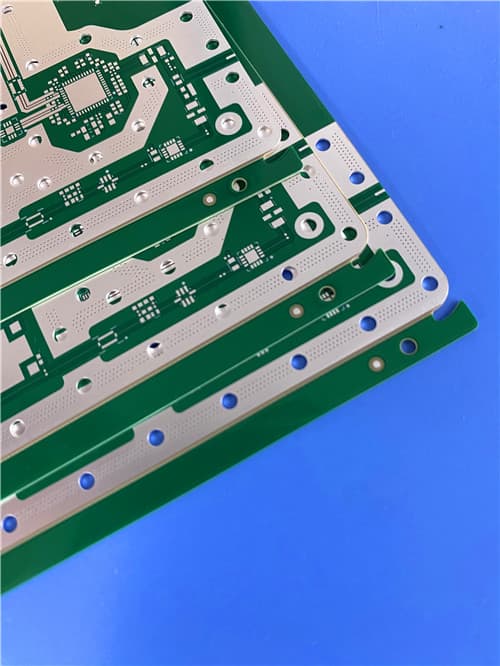
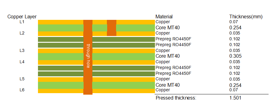
4. PCB Construction Details
| Item |
Specification |
| Product Type | 6-Layer High-Speed / RF PCB |
| Laminate Material | Isola I-Tera MT40 |
| Prepreg Material | Rogers RO4450F |
| Layer Count | 6 Layers |
| Outer Layer Copper | 2oz (approx. 70μm) |
| Inner Layer Copper | 1oz (approx. 35μm) |
| Finished Thickness | 1.501mm |
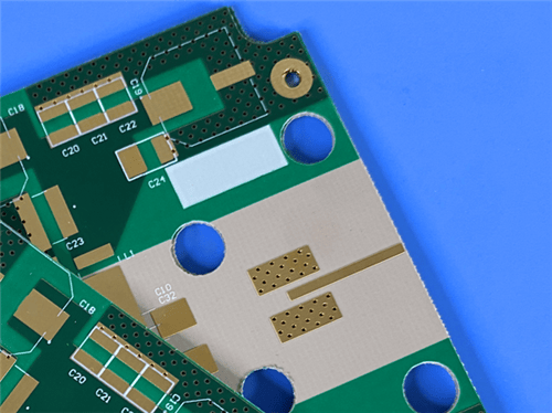
| Surface Finish | ENIG, Gold Thickness 2μ″ |
| Solder Mask | Green |
| Silkscreen | White |
| Impedance Control | 50Ω single-ended, TOP layer 5mil trace |
| Via Process | 0.3mm vias, resin-filled and plated over |
| Via Type | Blind vias |
| Special Feature | Edge plating (metal wrap-around) |
| Dimensions | 99mm x 99mm = 1 PC |
| Design Standard | IPC-Class-2 |
| Artwork Format | Gerber RS-274-X |
| Availability | Worldwide |
5. PCB Stackup (6-Layer Rigid Structure)
L1 (Top): 2oz Copper, 5mil traces for 50Ω single-ended impedance control
Dielectric: I-Tera MT40 core / RO4450F prepreg layers
L2: 1oz Copper
Dielectric: I-Tera MT40 core / RO4450F prepreg layers
L3: 1oz Copper
Dielectric: I-Tera MT40 core / RO4450F prepreg layers
L4: 1oz Copper
Dielectric: I-Tera MT40 core / RO4450F prepreg layers
L5: 1oz Copper
Dielectric: I-Tera MT40 core / RO4450F prepreg layers
L6 (Bottom): 2oz Copper
6. Primary Application Areas
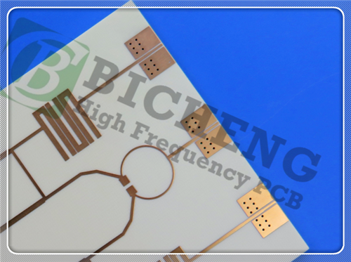
Commercial Airborne Antennas and broadband communication systems
Microstrip and Stripline Circuits for precision RF designs
Millimeter Wave Applications including 5G/6G infrastructure
Radar Systems for defense and automotive applications
Guidance Systems and aerospace navigation equipment
Point-to-Point Digital Radio Antennas for backhaul networks
Satellite Communications requiring low outgassing materials
Test and Measurement Equipment for high-frequency signal analysis
7. Quality Assurance
Artwork supplied: Gerber RS-274-X
Accepted standard: IPC-Class-2
Availability: Worldwide
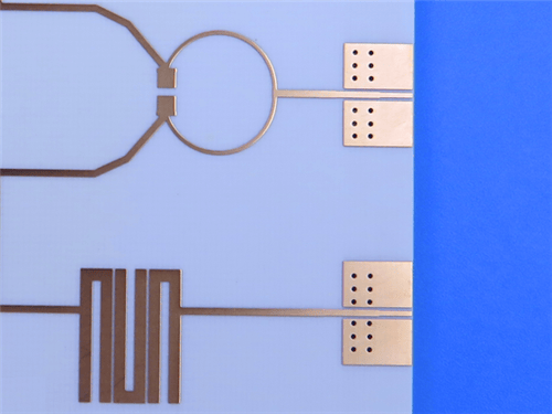
8. What is Single-Ended Impedance Control?
Single-ended impedance control refers to the precise management of the characteristic impedance of a signal trace referenced to a ground plane, without a paired differential trace. In high-speed digital and RF designs, signal traces must maintain a consistent impedance—typically 50Ω—to prevent reflections, signal degradation, and electromagnetic interference.
For the 5mil trace on the TOP layer of this PCB, the trace width, dielectric thickness, and material Dk (3.45) are carefully calculated to achieve 50Ω characteristic impedance. This ensures maximum power transfer and minimal signal distortion for high-frequency signals.
9. What is Edge Plating and Why Use It?
Edge plating (also known as side plating or edge metallization) is a process where the perimeter edges of a PCB are plated with copper and finished with the board's surface finish. This creates a conductive path along the board edges.
Benefits of edge plating:
EMI/RFI shielding: Creates a continuous Faraday cage around the board, reducing electromagnetic emissions and improving immunity
Enhanced grounding: Provides additional ground paths and low-impedance connections between layers
Thermal dissipation: Helps conduct heat away from the board edges
Mechanical protection: The plated edge protects the exposed substrate from moisture absorption and mechanical damage
Improved solderability: Enables edge connections for board-to-board or board-to-chassis mounting
Reduced parasitics: Minimizes edge effects in high-frequency designs
|