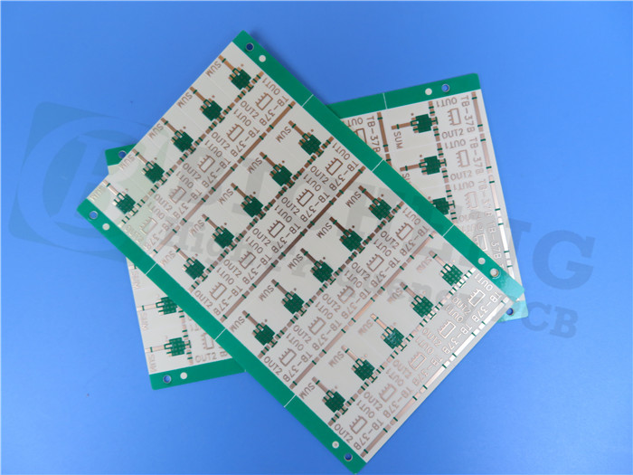
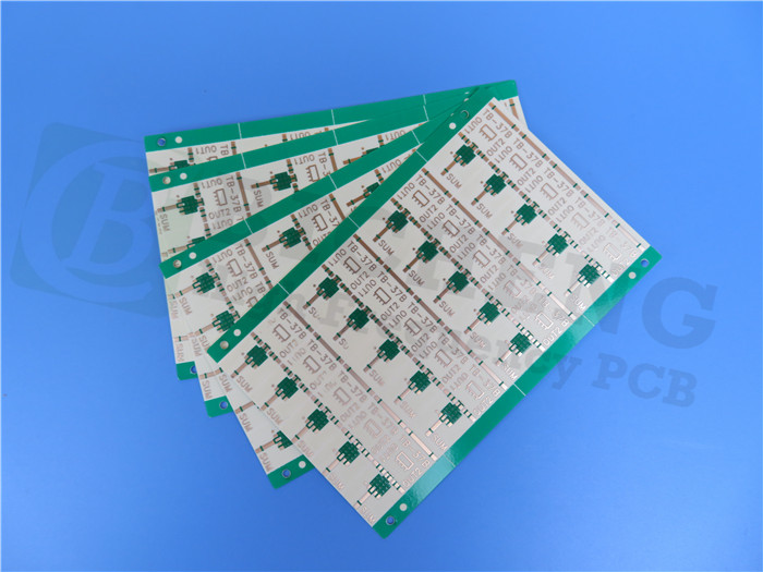
RO4725JXR Antenna PCB - Double Layer 30.7mil (0.78mm) Substrate with Immersion Gold Finish
(Printed Circuit Boards are custom-made products, the picture and parameters shown are just for reference)
Brief Introduction
The RO4725JXR Antenna PCB is a double-layer rigid circuit board designed for high-performance RF applications. Built on Rogers RO4725JXR substrates with a thickness of 30.7mil (0.78mm), this PCB features a finished board thickness of 0.9mm and 1oz copper on both outer layers. The board dimensions are 146.15mm x 60.8mm, with a minimum trace/space of 5/6 mils and a minimum hole size of 0.5mm. The surface finish is immersion gold, with a green solder mask on the top side and no solder mask on the bottom. The PCB is manufactured in compliance with IPC Class 2 standards and undergoes 100% electrical testing before shipment. It is supplied with Gerber RS-274-X files and is available worldwide.
PCB Specifications
| Parameters | Values |
| PCB Type | 2-layer rigid PCB |
| Copper_layer_1 | 35 μm |
| Rogers RO4725JXR Core | 30.7mil (0.780 mm) |
| Copper_layer_2 | 35 μm |
| Board Dimensions | 146.15mm x 60.8mm = 20PCS, +/- 0.15mm |
| Minimum Trace/Space | 5/6 mils |
| Minimum Hole Size | 0.5mm |
| Blind vias | No |
| Finished Board Thickness | 0.9mm |
| Finished Cu Weight | 1oz (1.4 mils) outer layers |
| Via Plating Thickness | 20 μm |
| Surface Finish | Immersion Gold |
| Top Silkscreen | No |
| Bottom Silkscreen | No |
| Top Solder Mask | Green |
| Bottom Solder Mask | No |
| Electrical Test | 100% prior to shipment |
| Components | 54 |
| Total Pads | 67 |
| Thru Hole Pads | 0 |
| Top SMT Pads | 67 |
| Bottom SMT Pads | 0 |
| Vias | 249 |
| Nets | 3 |
| Type of Artwork Supplied | Gerber RS-274-X |
| Quality Standard | IPC-Class-2 |
| Availability | Worldwide |
| Typical Applications | Cellular Base Station Antennas and Power Amplifiers |
Features & Benefits
1.Reduced Passive Intermodulation (PIM): Improves signal quality and reduces interference.
2.Low Insertion Loss: Minimizes signal loss during transmission, ensuring high efficiency.
3.Dielectric Constant (Dk) of 2.55: Ensures consistent electrical performance and compatibility with standard PTFE-based materials.
4.Low Density (1.27 g/cm³): Approximately 30% lighter than PTFE/Glass boards, offering weight savings.
5.Low Z-Axis CTE (25.6 ppm/°C): Ensures dimensional stability and reliable performance across temperature variations.
6.High Glass Transition Temperature (Tg > 280°C): Provides design flexibility and compatibility with automated assembly processes.
7.Low TCDk (+34 ppm/°C): Ensures consistent circuit performance, minimizing variations due to temperature changes.
8.Environmentally Friendly: Lead-free process compatible and RoHS compliant.
Typical Applications
1.Cellular Base Station Antennas
2.Power Amplifiers
PCB Capability (2023)
| Factory Process Capability (2023) | |
| Substrate Types and Brands | Standard FR-4, High Tg FR-4, High Frequency Materials, Polyimide/PET flexible Materials |
| Shengyi, ITEQ, Isola, Taiwan Union, Rogers Corp. Taconic, Panasonic | |
| Board Types | Rigid PCB, Flexible Circuits, Rigid-Flex PCB, Hybrid PCB, HDI PCB |
| CCL Model | High Tg FR-4: S1000-2M, TU-872 SLK, TU-768, IT-180A High CTI FR-4: S1600L, ST115 |
| Rogers Corp: RO4350B, RO4003C, RO4730G3, RO4360G2, RO4533, RO4534, RO4535, RO4835, RO3003, RO3006, RO3010, RO3035, RO3203, RO3210; RT/Duriod 5880; RT/Duriod 5870, RT/Duriod 6002, RT/Duroid 6010, RT/duroid 6035HTC; RT/duroid 5880LZ; TMM3, TMM4, TMM6, TMM10, TMM10i, TMM13i, Kappa 438; AD250C, AD255C, AD300D, AD350A, AD450, AD600, AD1000, TC350; TC600; DiClad 880, DiClad 870, DiClad 527; IsoClad 917 | |
| Taconic: TLF-35; RF-35TC, RF-60A, RF-60TC, RF-35A2, RF-45, RF-10, TRF-45; TLX-0, TLX-6, TLX-7, TLX-8; TLX-9, TLY-3, TLY-5, TLY-5Z; | |
| F4B PTFE Composites: (DK2.2 DK2.65 DK2.85 DK2.94, DK3.0, DK3.2, DK3.38, DK3.5, DK4.0, DK4.4, DK6.15, DK10.2) | |
| Maximum Delivery Size | 1200mm x 572 mm |
| Minimum Finished Board Thickness | L≤2L: 0.15mm; 4L: 0.4mm |
| Maximum Finished Board Thickness | 10.0 mm |
| Blind Buried Holes (Non-crossing) | 0.1mm |
| Maximum Hole Aspect Ratio | 15:01 |
| Minimum Mechanical Drill Hole Diameter | 0.1 mm |
| Through-hole Tolerance | +/- 0.0762 mm |
| Press-fit Hole Tolerance | +/- 0.05mm |
| Non-plated Copper Hole Tolerance | +/- 0.05mm |
| Maximum Number of Layers | 32 |
| Internal and External Layer Maximum Copper Thickness | 12Oz |
| Minimum Drill Hole Tolerance | +/- 2mil |
| Minimum Layer-to-Layer Tolerance | +/- 3mil |
| Minimum Line Width/Spacing | 3mil/3mil |
| Minimum BGA Diameter | 8mil |
| Impedance Tolerance | < 50Ω ±5Ω; ≥50Ω±10% |
| Surface Treatment Processes | Leaded/Lead-free HASL, Immersion Gold, Immersion Silver, Immersion Tin, OSP, ENIG, ENEPIG, Carbon Ink, Peelable Mask, Gold Finger, etc. |