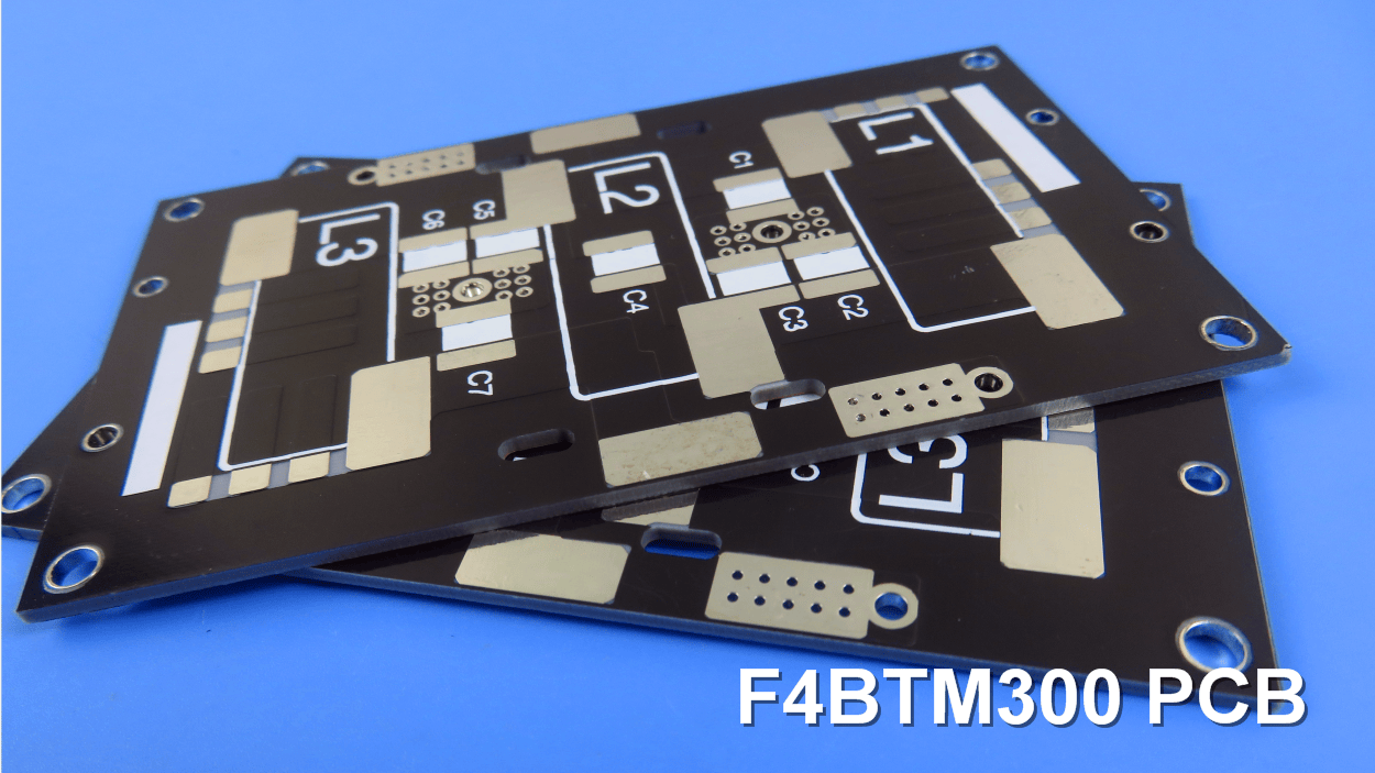
F4BTM High Frequency PCBs A Cost Effective PTFE Based Solution
 October 8, 2025
In the evolving world of high-frequency circuit design, the demand for materials that deliver both performance and cost efficiency is higher than ever. Wangling’s F4BTM series meets this need with a carefully engineered laminate that combines PTFE resin, fiberglass cloth, and nano-ceramic fillers to offer an ideal balance of electrical and mechanical properties.
Suitable for a wide range of commercial and industrial applications, F4BTM brings together low-loss performance, thermal reliability, and design flexibility—making it an excellent choice for high-volume and high-frequency projects.
What Is F4BTM?
F4BTM is a high-frequency laminate based on an F4BM dielectric layer enhanced with nano-ceramic fillers. This formulation results in:
Higher dielectric constant
Improved heat resistance
Lower thermal expansion coefficient
Higher insulation resistance
Better thermal conductivity
Maintained low-loss characteristics
The series includes two versions:
F4BTM: uses standard ED copper foil
F4BTME: uses reverse-treated foil (RTF) for improved PIM performance, finer line control, and reduced conductor loss
Both share the same high-performance dielectric base, giving designers the flexibility to choose based on application needs.
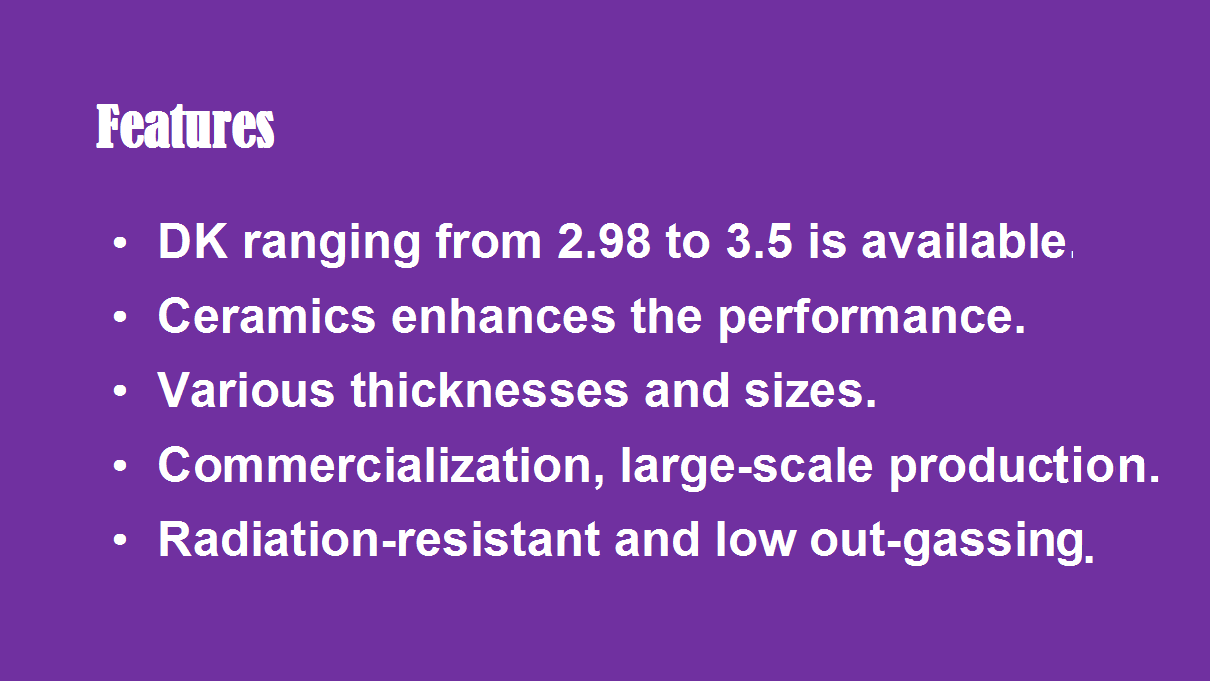
Key Features of F4BTM Laminates
Adjustable Dielectric Constant: Dk values ranging from 2.98 to 3.5
Thermal & Mechanical Stability: Excellent heat resistance and low CTE
Low Loss & High Insulation: Ideal for sensitive RF and microwave circuits
Space-Ready Performance: Radiation-resistant and low out-gassing properties
Scalable & Cost-Effective: Commercialized and ready for large-volume production
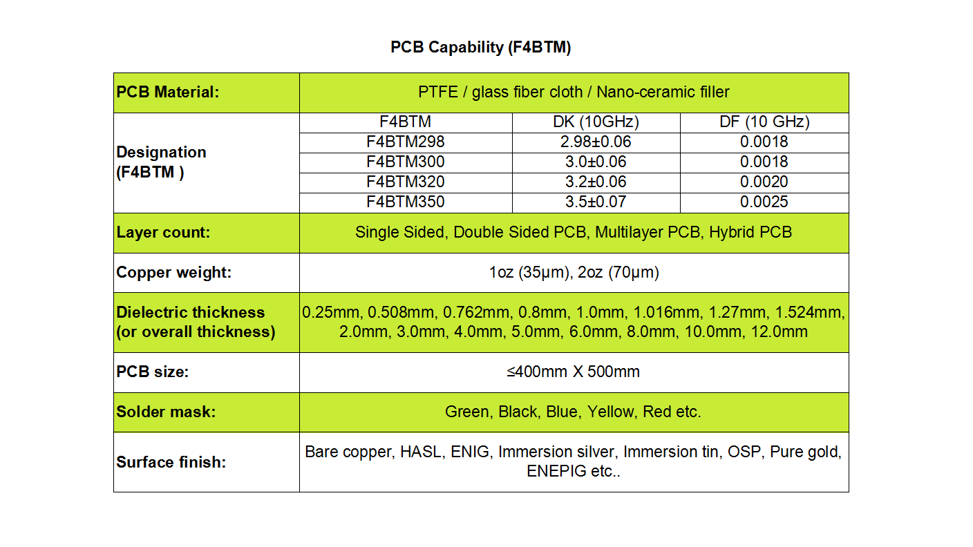
PCB Manufacturing Flexibility
We support full customization of F4BTM-based PCBs with the following options:
Layer Configurations: Single-sided, double-sided, multilayer, and hybrid builds
Copper Weight: 1 oz (35µm) and 2 oz (70µm)
Dielectric Thickness: From 0.25 mm up to 12.0 mm
Max Board Size: Up to 400 mm × 500 mm
Solder Mask Colors: Green, black, blue, yellow, red, and more
Surface Finishes: HASL, ENIG, Immersion Silver, Immersion Tin, OSP, Pure Gold, ENEPIG, and bare copper
Common Applications
F4BTM PCBs are used across a variety of high-frequency and wireless technologies, including:
Antennas
Mobile internet devices
Sensor networks
Radar and millimeter-wave radar systems
Aerospace and satellite navigation
Power amplifiers
Conclusion
Whether you're developing communication systems, radar modules, or IoT devices, F4BTM offers a reliable and cost-efficient substrate that doesn’t compromise on performance. Its combination of PTFE flexibility, ceramic-enhanced stability, and scalable manufacturing makes it a go-to material for next-generation RF designs.
Interested in learning how F4BTM can optimize your next high-frequency project? Contact us to explore design support and prototyping options.