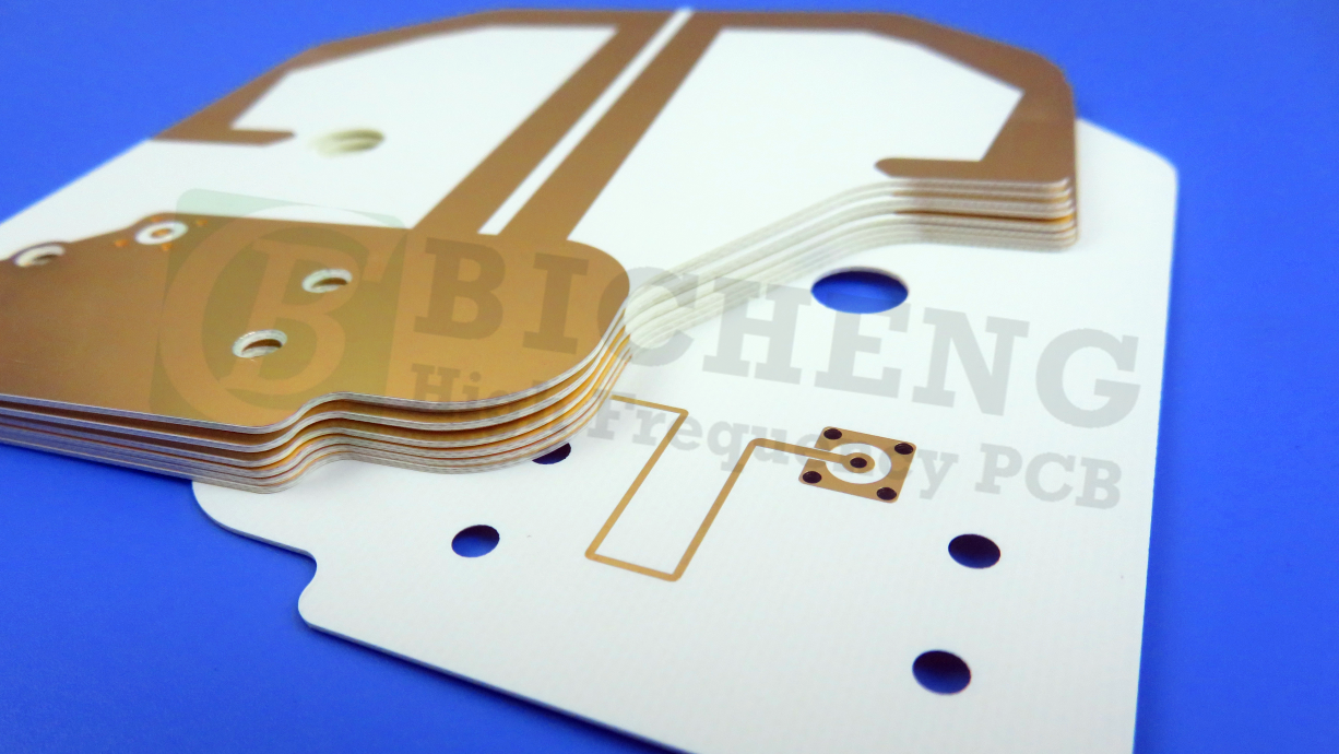
High-Performance RO4360G2 2-Layer PCB for Telecommunications and Power Applications1. Introduction to RO4360G2 The RO4360G2 laminate is a low-loss, glass-reinforced, hydrocarbon ceramic-filled thermoset material that offers an optimal balance of performance and processing capability. As the first high dielectric constant (Dk) thermoset laminate that can be processed similarly to conventional FR-4, RO4360G2 provides enhanced rigidity for improved processability in multi-layer board constructions. This material is lead-free process capable and helps reduce both material and fabrication costs. It can be effectively paired with RO440 series prepreg and lower-Dk RO4000 laminates in multi-layer designs. 2. Features and Benefits Features Benefits Design Flexibility: Allows for versatile applications in various circuit designs.
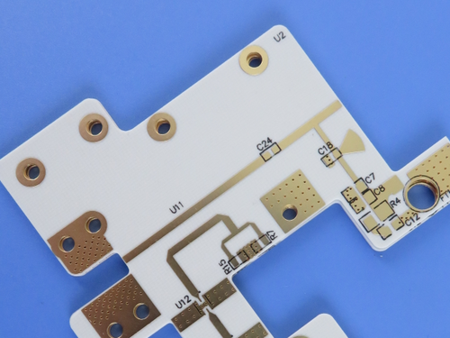
3. PCB Construction Details
4. PCB Stackup Copper Layer 1: 35 µm 5.PCB Statistics Components: 18 6.Manufacturing & Compliance Artwork Format: Gerber RS-274-X 7.Typical Applications Base station power amplifiers |
Get a Quick Quote
Fill in the form below and our engineers will reply within 24 hours with technical specifications and pricing for High-Performance RO4360G2 2-Layer PCB for Telecommunications and Power Applications.
.jpg)
.jpg)
.jpg)
.jpg)
.jpg)
.jpg)