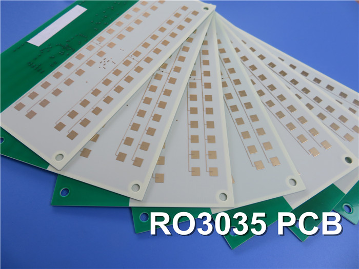
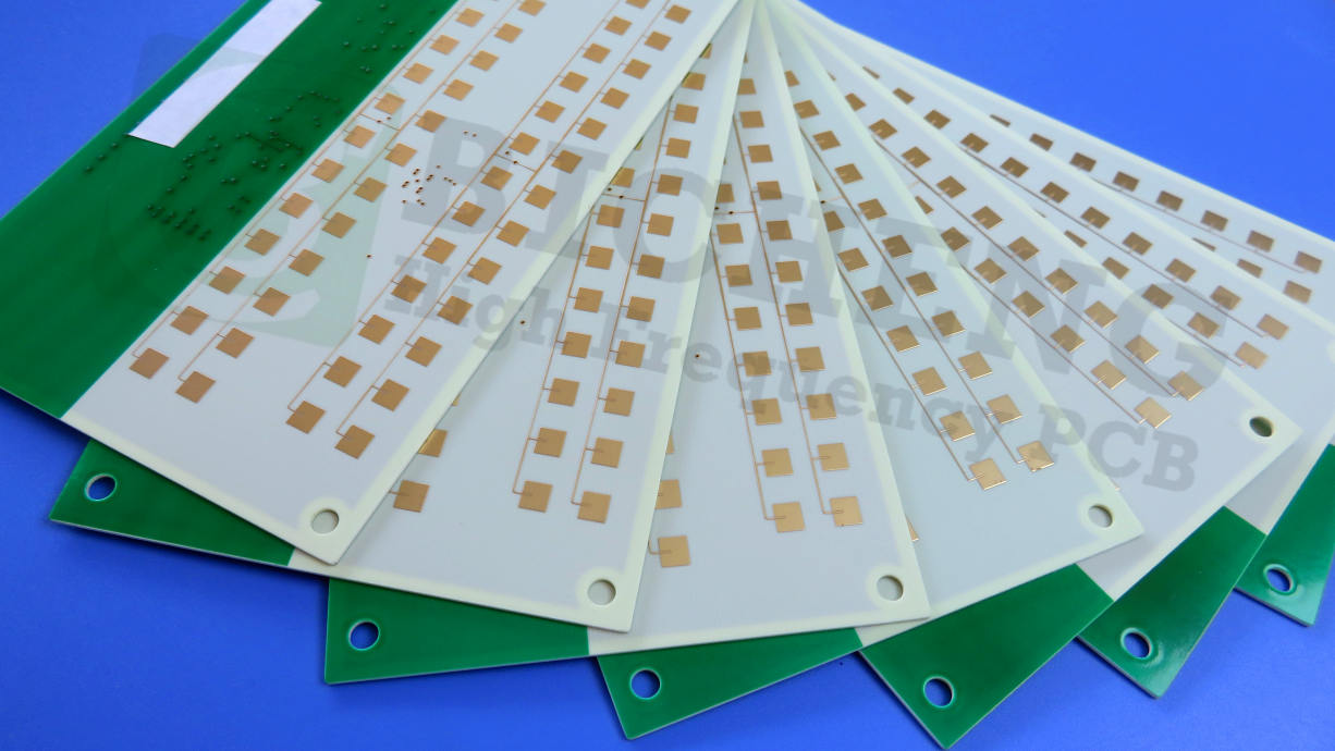
RO3035 2-Layer PCB with Immersion Gold for High-Frequency Applications
1. Introduction to RO3035
The RO3035 laminate is a ceramic-filled, PTFE-based material designed for high-frequency circuit applications. It belongs to the RO3000 series, which offers mechanically similar materials with varying dielectric constants (Dk). This allows for the development of multi-layer board designs without compromising warping or reliability. The RO3035 laminate maintains a stable dielectric constant across a range of temperatures, making it suitable for applications in 5G, millimeter-wave sub-6 GHz, and massive MIMO systems.
2. Features and Benefits
Features
Material Composition: Rogers RO3035 ceramic-filled PTFE composites.
Dielectric Constant: 3.5 ± 0.05 at 10 GHz and 23°C.
Dissipation Factor: 0.0015 at 10 GHz and 23°C.
Thermal Properties: Td > 500°C; thermal conductivity of 0.5 W/mK.
Moisture Absorption: Low at 0.04%.
Coefficient of Thermal Expansion (CTE): X-axis: 17 ppm/°C, Y-axis: 17 ppm/°C, Z-axis: 24 ppm/°C (within -55 to 288°C).
Benefits
Frequency Range: Suitable for applications up to 30-40 GHz.
Reliability: Lower operating temperatures and increased reliability in power amplifiers.
Mechanical Properties: Uniform properties for a variety of dielectric constants, ideal for multi-layer board designs.
Thermal Expansion: Low in-plane expansion coefficient, ensuring reliable surface-mounted assemblies, especially in temperature-sensitive applications.
Dimensional Stability: Excellent stability under varying conditions.
Cost-Effective Manufacturing: Economical laminate pricing for volume production.
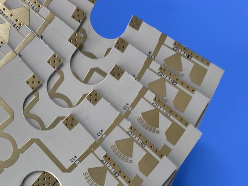
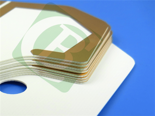
3. PCB Construction Details
| Parameter | Specification |
|---|
| Base Material | RO3035 |
| Layer Count | 2 layers |
| Board Dimensions | 67.1 mm x 57.6 mm (2 types, 2 pieces each) |
| Minimum Trace/Space | 4/5 mils |
| Minimum Hole Size | 0.2 mm |
| Blind Vias | None |
| Finished Board Thickness | 0.2 mm |
| Finished Copper Weight | 1 oz (1.4 mils) on outer layers |
| Via Plating Thickness | 20 µm |
| Surface Finish | Immersion gold |
| Solder Mask | None on both top and bottom sides |
| Silkscreen | None on both top and bottom sides |
| Electrical Testing | 100% electrical test conducted prior to shipment |
4. PCB Stackup
Copper Layer 1: 35 µm
RO3035 Substrate: 5 mil (0.127 mm)
Copper Layer 2: 35 µm
5.PCB Statistics
Components: 39
Total Pads: 82
Thru Hole Pads: 52
Top SMT Pads: 30
Bottom SMT Pads: 0
Vias: 51
Nets: 2
6.Manufacturing & Compliance
Artwork Format: Gerber RS-274-X
Quality Standard: IPC-Class-2 compliant
Availability: Worldwide production and shipping
7.Typical Applications
Automotive radar applications
Global positioning satellite antennas
Cellular telecommunications systems, including power amplifiers and antennas
Patch antennas for wireless communications
Direct broadcast satellites
Datalink on cable systems
Remote meter readers
Power backplanes
|
.jpg)
.jpg)
.jpg)