News that NVIDIA RTX 5090 graphics card adopts 14-layer PCB
 December 31, 2024
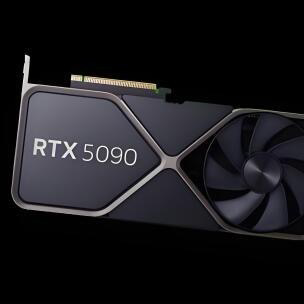
December 30 News: Last week, the bare PCB and test sample PCB of NVIDIA Corporation's GeForce RTX 5090 graphics card were exposed. Taiwanese media BenchLife.info has provided more information about this flagship gaming graphics card from the Blackwell generation.
The media reports that the RTX 5090 will feature a 14-layer PCB design, expected to utilize a 16+6+7 phase power supply configuration, although it is unclear whether this refers to NVIDIA's reference design for third parties or the Founders Edition (FE) version. For reference, the previous generation RTX 4090 FE used a 20+3 phase power supply.
Reports indicate that the NVIDIA GeForce RTX 5090 graphics card will have a TGP (Total Graphics Power) of up to 600W. Additionally, the RTX 50 series graphics cards, starting from the RTX 5070 with a TGP of 200W or higher, will utilize a 12V-2×6 power connector.
The RTX 5090 is based on the GPU core variant codenamed GB202-300-A1, featuring 170 SMs (which translates to 21,760 CUDA cores), equipped with 32GB of GDDR7 memory on a 512-bit wide bus, and utilizing a PCIe 5.0×16 interface.