12-Layer Through Holes PCB for High-Performance Applications
(Custom PCBs are tailored products; the images and specifications provided are for reference only.)
Introduction of IT-180ATC
IT-180ATC is an advanced high Tg (175°C by DSC) multifunctional filled epoxy known for its high thermal reliability and CAF resistance. This material is suitable for various applications and can withstand lead-free assembly temperatures of up to 260°C.
Features of IT-180ATC
Dielectric Constant: DK of 4.1 at 10 GHz
Dissipation Factor: 0.017 at 10 GHz
Thermal Resistance: T260 > 60 minutes, T288 > 20 minutes
Peel Strength: Minimum standard ED copper of 8 lbs/inch
Coefficient of Thermal Expansion (CTE): Matched to copper with X-axis of 11-13 ppm/°C and Y-axis of 13-15 ppm/°C
Z-axis CTE: Low at 45 ppm/°C
Tg: Greater than 175°C
Moisture Absorption: Low at 0.1%
Flammability Rating: UL 94-V0
Basic PCB Specifications
Material Type: IT-180A, FR-4 Tg170°C
Layer Count: 12 layers
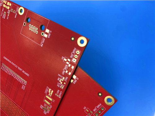
Solder Mask: Both sides, Matt Red
Silkscreen Print: Top side, white
Surface Finish: ENIG
Total Board Thickness: 1.6 mm ± 10%
Board Size: 80.15 mm x 76.6 mm (1 PCS)
Minimum Hole Size: 0.2 mm
Solder Mask Thickness: 10 µm
Minimum Dielectric Thickness: 100 µm
Minimum Trace Line Width: 120 µm
Minimum Spacing: 125 µm
Plated Through Holes: L1-L12
Blind and Buried Vias: L1-L5, L7-L10, L7-L12
Impedance Controlled:
50 ohm, differential pairs, Top layer, 4 mil / 4 mil trace/gap, reference layer 2
90 ohm, differential pairs, Top layer, 5 mil / 6 mil trace/gap, reference layer 2
100 ohm, differential pairs, Top layer, 6 mil / 9 mil trace/gap, reference layer 2
50 ohm, differential pairs, Layer 3, 5 mil / 5 mil trace/gap, reference layer 2, Layer 4
90 ohm, differential pairs, Layer 5, 7 mil / 6 mil trace/gap, reference layer 4, Layer 6
100 ohm, differential pairs, Layer 8, 6 mil / 6 mil trace/gap, reference layer 7, Layer 9
All 0.2 mm and 0.3 mm vias are filled and capped according to IPC 4761 Type VII. A printing series number is required.
PCB Stack-Up (Component Side at Top)
| TYPE | LAYER NO. | THICKNESS (µm) | SPECIFICATION |
|---|---|---|---|
| COPPER | 1 | 45 | 18 µm BASE COPPER + 25 µm PLATING |
| FR-4 | PP | 150 | IPC-4101/24 |
| COPPER | 2 | 17 | |
| FR-4 IT-180 | Core | 135 | IPC-4101/24 |
| COPPER | 3 | 17 | |
| FR-4 | PP | 153 | IPC-4101/24 |
| COPPER | 4 | 17 | |
| FR-4 IT-180 | Core | 115 | IPC-4101/24 |
| COPPER | 5 | 17 | |
| FR-4 | PP | 94 | IPC-4101/24 |
| COPPER | 6 | 17 | |
| FR-4 IT-180 | Core | 115 | IPC-4101/24 |
| COPPER | 7 | 17 | |
| FR-4 | PP | 94 | IPC-4101/24 |
| COPPER | 8 | 17 | |
| FR-4 IT-180 | Core | 115 | IPC-4101/24 |
| COPPER | 9 | 17 | |
| FR-4 | PP | 150 | IPC-4101/24 |
| COPPER | 10 | 17 | |
| FR-4 IT-180 | Core | 135 | IPC-4101/24 |
| COPPER | 11 | 17 | |
| FR-4 | PP | 150 | IPC-4101/24 |
| COPPER | 12 | 45 | 18 µm BASE COPPER + 25 µm PLATING |
PCB Statistics
Components: 240
Total Pads: 482
Thru Hole Pads: 234
Top SMT Pads: 138
Bottom SMT Pads: 110
Vias: 256
Nets: 10
Standards and Availability
Artwork Type: Gerber RS-274-X
Accepted Standard: IPC-Class-2
Availability: Worldwide
Typical Applications
Automotive (Engine Room ECU)
Backplanes
Data Storage
Server and Networking
Telecommunications
