IT-180 10-Layer High Temperature HDI PCB with Immersion Gold and 100 Ohm Impedance
(All PCBs are custom-manufactured. Reference images and parameters may vary based on your design requirements.)
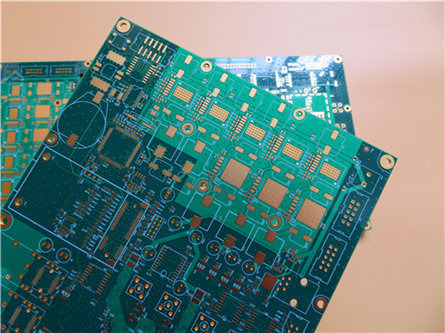
Brief Introduction
This 10-layer printed circuit board is constructed using ITEQ’s IT-180 FR-4 Tg170 substrate, specifically designed for PLC control applications. It has a thickness of 2.0 mm, featuring a white silkscreen on a green solder mask and immersion gold coating on the pads. The board is supplied as a single unit and incorporates a high-density interconnection configuration with blind vias from layers L1 to L3 and L7 to L10, as well as buried vias from L3 to L7. A 100 ohm impedance is controlled on the top layer with trace/gap dimensions of 4 mil/5 mil. The boards are fabricated according to IPC 6012 Class 2 standards using the provided Gerber data, with each set of 20 boards vacuum packed for shipment.
PCB Specifications
| Item | Description | Value | |
| Layer count | 10 layer PCB | 10 layer board | |
| Board type | Multilayer pcb | Multilayer pcb board | |
| Board size | 168.38 x 273.34mm=1up | 168.38 x 273.34mm=1up | |
| Laminate | Laminate Type | FR4 IT-180A | |
| Supplier | ITEQ | ||
| Tg | TG ≧170 | ||
| Finished thickness | 2.0+/-10% MM | ||
| Plating Thickness | PTH Cu thickness | >20 um | |
| Inner layer Cu Thickness | 1/1 OZ | ||
| Surface Cu thickness | 35 um | ||
| Solder Mask | Material type | LP-4G G-05 | |
| Supplier | Nan Ya | ||
| Color | Green | ||
| Single / both sides | Both Sides | ||
| S/M thickness | >=10.0 um | ||
| 3M tape test | NO Peel Off | ||
| Legend | Material type | S-380W | |
| Supplier | Tai yo | ||
| Color | White | ||
| Location | Both Sides | ||
| 3M tape test | No peel off | ||
| Circuit | Trace Width (mm) | 0.203+/-20%mm | |
| Spacing (mm) | 0.203+/- 20%mm | ||
| Identification | UL mark | 94V-0 | |
| Date code | 1025 | ||
| Mark location | CS | ||
| Surface Treatment | ENIG | Nickel | 100u'' |
| Gold | ≧2u'' | ||
| Reliabilty Tests | Thermal shock test | 288±5℃, 10sec ,3 cycles | |
| solder abllity test | 245±5℃ | ||
| Function | Electrioal Test | 233+/-5℃ | |
| Standard | IPC_6012C CLASS 2 | 100% | |
| Appearance | Visual inspection | 100% | |
| warp and twist | <= 0.75% | ||
| Vias | Through holes | L1-L10 | |
| Blind vias & Buried vias | L1-L3, L7-L10, L3-L7 | ||
| Drill table (mm) | No | PTH/NPTH | Size |
| 1 | Y | 0.500*1.00+/-0.075 | |
| 2 | Y | 0.508+/-0.075 | |
| 3 | Y | 0.610+/-0.075 | |
| 4 | N | 0.700+/-0.075 | |
| 5 | Y | 0.711+/-0.075 | |
| 6 | Y | 0.914+/-0.075 | |
| 7 | N | 1.118+/-0.075 | |
| 8 | N | 1.219+/-0.075 | |
| 9 | N | 1.524+/-0.075 | |
| 10 | N | 1.600+/-0.075 | |
| 11 | Y | 2.540+/-0.075 | |
| 12 | Y | 2.997+/-0.075 | |
| 13 | N | 3.500+/-0.075 | |
Typical Applications
CCTV Security: Suitable for security camera systems.
Wireless G Router: Designed for wireless communication devices.
Programmable Controllers: Ideal for automation applications.
Automotive: Used in engine room ECU systems.
Multilayer and HDI PCB: Supports complex circuit designs.
Backplanes: Suitable for high-performance backplane applications.
Data Storage: Designed for data storage solutions.
Server and Networking: Meets the demands of server and networking equipment.
Telecommunications: Ideal for telecom devices.
Our Advantages
Proactive Engineering Design: Prevents issues during pre-production.
Certifications: ISO9001, ISO14001, ISO13485, IATF 16949, UL certified.
Robust PCB Capabilities: Supports R&D, sales, and marketing efforts.
Any Layer HDI PCBs: Flexible production options available.
Workshop Size: 16,000㎡ facility with a monthly output of 30,000㎡.
Diverse PCB Types: Capable of producing 8,000 types of PCBs monthly.
Customer Satisfaction: Complaint rate of less than 1%.
Timely Delivery: Quick and reliable shipping.
No Minimum Order Quantity: Low cost for prototypes and small runs.
Experience: Over 22 years in high-frequency PCB manufacturing.
