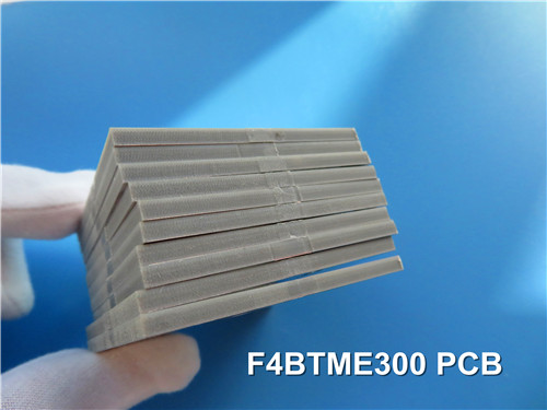
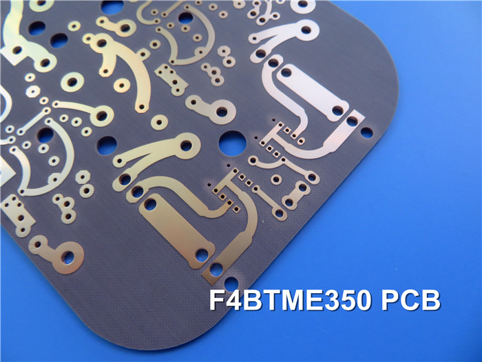
F4BTME350 High Frequency PCB PTFE RF Circuit Board with Immersion Gold
(Printed Circuit Boards are custom-made products; the images and specifications provided are for reference only.)
1. Introduction to F4BTME350 High Frequency PCB
The F4BTME series laminates are manufactured through a meticulous process that involves the scientific formulation of glass fiber cloth, nano-ceramic fillers, and polytetrafluoroethylene (PTFE) resin.
These substrates are built upon the F4BM dielectric layer and incorporate high dielectric constant and low loss nano-ceramics. This integration results in enhanced dielectric constant, superior heat resistance, reduced thermal expansion coefficient, increased insulation resistance, and improved thermal conductivity, all while maintaining low loss characteristics.
Furthermore, F4BTME laminates are specifically paired with reverse-treated RTF copper foil, providing exceptional performance in terms of PIM, precise line control, and minimized conductor loss.
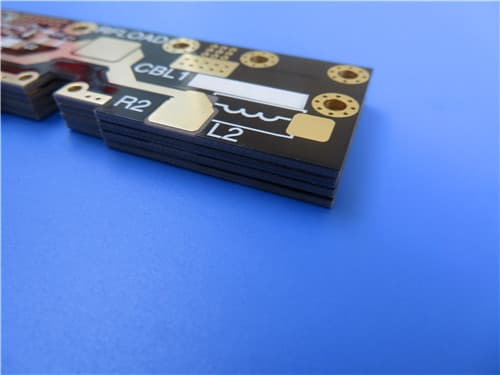
This 2-layer rigid PCB is constructed entirely with F4BTME350 as the core material at 10mil (0.254mm) thickness, with immersion gold surface finish, black top solder mask, white top silkscreen, and 1oz RTF copper on both sides. Its DK of 3.5 offers excellent high-frequency performance, making it ideal for demanding applications such as 4G/5G base station antennas, LNAs, LNBs/LNCs, phased array antennas, satellite communications, and radar systems.
2. Key Features of F4BTME350 PCB
Dielectric Constant (DK): 3.5 ± 0.07 at 10GHz
Dissipation Factor (Df): 0.0025 at 10GHz / 0.0035 at 20GHz
TCDK: -60 ppm/°C (-55°C to 150°C)
CTE: X-axis 10 ppm/°C, Y-axis 12 ppm/°C, Z-axis 51 ppm/°C (-55°C to 288°C)
Thermal Conductivity: 0.54 W/(M·K)
Moisture Absorption: ≤0.05%
PIM Value: ≤ -160 dBc (F4BTME only)
Peel Strength (1oz F4BTME): >1.4 N/mm
Volume Resistivity: ≥1×10⁷ MΩ·cm
Surface Resistivity: ≥1×10⁶ MΩ
Electrical Strength (Z direction): >32 KV/mm
Breakdown Voltage (XY direction): >40 KV
Density: 2.20 g/cm³
Long-term Operating Temperature: -55°C to +260°C
UL 94 V-0 Flammability Rating
Radiation resistance and low outgassing
3. Benefits of F4BTME350 PCB
Stable DK (3.5±0.07) — Consistent impedance control for high-frequency designs
Low Df (0.0025 @ 10GHz) — Excellent signal integrity with minimal insertion loss
Excellent PIM Performance (≤ -160 dBc) — Critical for low intermodulation distortion systems
Low CTE (10/12/51 ppm/°C) — Exceptional dimensional stability, matched to copper
High Thermal Conductivity (0.54 W/mK) — Superior heat dissipation for high-power applications
Nano-Ceramic Filled PTFE — Enhanced dielectric constant, reduced thermal expansion
RTF Copper Foil — Reduced conductor loss, excellent peel strength, precise line control
Radiation Resistance & Low Outgassing — Suitable for aerospace applications
Immersion Gold Finish — Excellent solderability, corrosion resistance, and wire bondability
4. PCB Construction Details
| Item | Specification |
|---|---|
| Base material | Wangling F4BTME350 (PTFE + Nano-Ceramic + Glass Fiber + RTF Copper) |
| Layer count | 2 layers |
| Board dimensions | 89.77mm x 45.16mm = 1 PCS, ±0.15mm |
| Minimum Trace/Space | 6/8 mils |
| Minimum Hole Size | 0.25mm |
| Blind vias | No |
| Finished board thickness | 0.3mm |
| Finished Cu weight | 1 oz (35 μm / 1.4 mils) all layers |
| Via plating thickness | 20 μm |
| Surface finish | Immersion Gold |
| Top Silkscreen | White |
| Bottom Silkscreen | No |
| Top Solder Mask | Black |
| Bottom Solder Mask | No |
| 100% Electrical test | Used prior to shipment |
5. PCB Stackup (2-Layer Rigid Structure)
Layer: Copper_layer_1 (Top), Material: Copper (RTF), Thickness: 35 μm (1 oz)
Layer: Dielectric, Material: F4BTME350 Core, Thickness: 0.254 mm (10mil)
Layer: Copper_layer_2 (Bottom), Material: Copper (RTF), Thickness: 35 μm (1 oz)
6. PCB Statistics
Components: 12
Total Pads: 38
Thru Hole Pads: 17
Top SMT Pads: 21
Bottom SMT Pads: 0
Vias: 9
Nets: 2
7. Wangling F4BTME350 Material – Product Introduction
The F4BTME series laminates are manufactured through a meticulous process that involves the scientific formulation of glass fiber cloth, nano-ceramic fillers, and polytetrafluoroethylene (PTFE) resin.
These substrates are built upon the F4BM dielectric layer and incorporate high dielectric constant and low loss nano-ceramics. This integration results in enhanced dielectric constant, superior heat resistance, reduced thermal expansion coefficient, increased insulation resistance, and improved thermal conductivity, all while maintaining low loss characteristics.
Furthermore, F4BTME laminates are specifically paired with reverse-treated RTF copper foil, providing exceptional performance in terms of PIM, precise line control, and minimized conductor loss.
F4BTME350 features a dielectric constant of 3.5±0.07 at 10GHz, dissipation factor of 0.0025 at 10GHz and 0.0035 at 20GHz, along with excellent thermal stability. The material operates reliably across a wide temperature range from -55°C to +260°C and is suitable for high-reliability RF and microwave applications.
8. Features and Benefits Summary
| Feature | Benefit |
|---|---|
| DK 3.5 ± 0.07 @ 10GHz | Stable dielectric constant for consistent impedance control |
| Df 0.0025 @ 10GHz | Low loss for high-frequency RF and microwave designs |
| Excellent PIM (≤ -160 dBc) | Ideal for low intermodulation distortion systems |
| TCDK: -60 ppm/°C | Stable electrical performance over temperature |
| CTE: 10/12/51 ppm/°C | Excellent dimensional stability and reliable plated through holes |
| Thermal conductivity 0.54 W/m/K | Efficient heat removal for high-power applications |
| Nano-ceramic filled PTFE | Enhanced dielectric constant and reduced thermal expansion |
| RTF copper foil | Reduced conductor loss, precise line control |
| Radiation resistance & low outgassing | Ideal for aerospace, satellite, and defense applications |
| Immersion Gold finish | Excellent solderability, corrosion resistance, wire bondability |
9. F4BTME350 Typical Properties (Data Sheet)
| Property | Typical Value | Condition | Unit | Test Method |
|---|---|---|---|---|
| Electrical Properties | ||||
| Dielectric Constant (Typical) | 3.5 ± 0.07 | 10 GHz | — | GB/T 12636-1990 / IPC-TM-650 2.5.5.5 Stripline |
| Dissipation Factor | 0.0025 | 10 GHz | — | GB/T 12636-1990 |
| Dissipation Factor | 0.0035 | 20 GHz | — | GB/T 12636-1990 |
| TCDK | -60 | -55°C ~ 150°C | ppm/°C | — |
| Volume Resistivity | ≥1×10⁷ | Normal State | MΩ·cm | IPC-TM-650 |
| Surface Resistivity | ≥1×10⁶ | Normal State | MΩ | IPC-TM-650 |
| Electrical Strength (Z direction) | >32 | 5KW, 500V/s | KV/mm | IPC-TM-650 2.5.6.2 |
| Breakdown Voltage (XY direction) | >40 | 5KW, 500V/s | KV | IPC-TM-650 |
| PIM Value | ≤ -160 | F4BTME only | dBc | — |
| Thermal Properties | ||||
| CTE (X-axis) | 10 | -55°C ~ 288°C | ppm/°C | IPC-TM-650 2.4.41 |
| CTE (Y-axis) | 12 | -55°C ~ 288°C | ppm/°C | IPC-TM-650 2.4.41 |
| CTE (Z-axis) | 51 | -55°C ~ 288°C | ppm/°C | IPC-TM-650 2.4.41 |
| Thermal Stress | No Delamination | 260°C, 10s, 3 times | — | IPC-TM-650 |
| Thermal Conductivity | 0.54 | Z direction | W/(M·K) | — |
| Long-Term Operating Temp | -55 ~ +260 | — | °C | — |
| Mechanical & Physical Properties | ||||
| Peel Strength (1oz F4BTME) | >1.4 | RTF Copper Foil | N/mm | IPC-TM-650 2.4.8 |
| Water Absorption | ≤0.05 | 20±2°C, 24 hours | % | ASTM D570 |
| Density | 2.20 | Room Temperature | g/cm³ | — |
| Flammability | V-0 | UL-94 | Grade | UL 94 |
| Material Composition | ||||
| Composition | PTFE + Glass Fiber + Nano-Ceramic (RTF Copper) | |||
10. Primary Application Areas
Base station antennas for 4G/5G communications
Low Noise Amplifiers (LNAs), Low Noise Block downconverters (LNBs/LNCs)
Phased array antennas, phase-sensitive antennas
Satellite communications, aerospace and cabin equipment
Microwave and RF modules, radar systems (including automotive radar)
High-power amplifiers, passive components (e.g., power dividers, couplers, combiners)
PCS/PCN large-format antennas, feed networks
11. Quality Assurance
Type of artwork supplied: Gerber RS-274-X
Accepted standard: IPC-Class-2
Availability: Worldwide
100% Electrical test prior to shipment
12. Standard Thickness, Panel Sizes & Claddings
Note: F4BTME350 minimum thickness is 0.254mm. The following thicknesses are available as either total thickness including copper or dielectric thickness. Please specify when ordering.
| Parameter | Options |
|---|---|
| Standard Dielectric Thicknesses (mm) | 0.254 (min), 0.508, 0.762, 0.8, 1.0, 1.016, 1.27, 1.524, 2.0, 3.0, 4.0, 5.0, 6.0, 8.0, 10.0, 12.0 |
| Thickness Tolerances (mm) | 0.254: ±0.02, 0.508: ±0.04, 0.762: ±0.05, 0.8: ±0.05, 1.0: ±0.05, 1.016: ±0.05, 1.27: +0.06, 1.524: ±0.06, 2.0: ±0.075, 3.0: ±0.09, 4.0: ±0.1, 5.0: ±0.1, 6.0: ±0.12, 8.0: ±0.15, 10.0: ±0.18, 12.0: ±0.2 |
| Standard Panel Sizes | 460×610mm, 600×500mm, 914×1220mm (Note: thickness ≥4.0mm cannot provide 914×1220mm) |
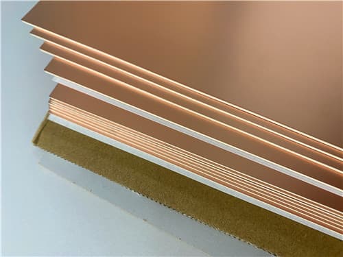
| Standard Claddings (F4BTME) | Reverse-treated RTF Copper: 0.5oz (18μm), 1oz (35μm) |
| Standard Claddings (F4BTM) | ED Copper: 0.5oz (18μm), 1oz (35μm), 1.5oz (50μm), 2oz (70μm) |
| DK Options (F4BTME Series) | 2.98, 3.0, 3.2, 3.5 |
| Metal Base Options | F4BTM(E)***-AL (Aluminum base), F4BTM(E)***-CU (Copper base) for shielding/heat dissipation |
13. F4BTM & F4BTME Series Aluminum/Copper Base Option
The F4BTM and F4BTME series can also be provided with an aluminum or copper base, where one side of the dielectric layer is covered with copper foil and the other side is laminated with copper or aluminum for shielding or heat dissipation purposes. Model designation: F4BTM***-AL, F4BTME***-AL, F4BTM***-CU, or F4BTME***-CU.
| Model | Metal Base | Specific Gravity | Thermal Conductivity | Available Metal Thickness | Thickness Tolerance | Available Sizes |
|---|---|---|---|---|---|---|
| F4BTM(E)-2-A***-CU | Copper (Purple/Brass) | 8.9 | 380 W/(M·K) | 0.48, 0.98, 1.48, 1.98, 2.98, 3.98mm (other thicknesses available upon request) | +0.02, -0.05 | 460×610mm, 460×305mm |
| F4BTM(E)-2-A***-AL | Aluminum | 2.7 | 180 W/(M·K) | 0.48, 0.98, 1.48, 1.98, 2.98, 3.98mm (other thicknesses available upon request) | +0.02, -0.05 | 460×610mm, 460×305mm |
Example: F4BTM300-AL represents F4BTM300 with aluminum base. F4BTME350-CU represents F4BTME350 with copper base.
14. Data Source Notes
Dielectric Constant (Typical) is tested in the Z-direction of the material using GB/T 12636-1990 or IPC-TM-650 2.5.5.5 Stripline method.
Other properties are tested using or referencing IPC-TM-650 or GBT4722-2017 standard test methods.
All test data are typical measurement values intended to assist customers in material selection. They do not constitute any express or implied warranty and do not guarantee performance in specific applications. Customers are responsible for verifying the suitability of Wangling materials for each application.
Get a Quick Quote
Fill in the form below and our engineers will reply within 24 hours with technical specifications and pricing for F4BTME350 2-Layer 0.3mm Immersion Gold High Frequency PCB.
.jpg)