Advanced 8-Layer HDI Hybrid PCBs Utilizing RO4003C and S1000-2M for High-Frequency Applications
(Custom PCBs are tailored products; the images and specifications provided are for reference only.)
Introduction of RO4003C
Rogers RO4003C materials are woven glass reinforced hydrocarbon/ceramics that provide the high-frequency performance of PTFE with the manufacturability of epoxy/glass. This low-loss material is suitable for RF microwave circuits and matching networks, allowing for competitive circuit fabrication.
RO4003C laminates are available in various configurations, using both 1080 and 1674 glass fabric styles, all meeting strict electrical performance specifications. The material is non-brominated and not UL 94 V-0 rated.
Features of RO4003C
Dielectric Constant: 3.38 ± 0.05 at 10 GHz
Dissipation Factor: 0.0027 at 10 GHz
Thermal Conductivity: 0.71 W/m/K
Thermal Coefficient of Dielectric Constant: +40 ppm/°C (range -50°C to 150°C)
CTE Matched to Copper: X-axis: 11 ppm/°C, Y-axis: 14 ppm/°C
Low Z-axis CTE: 46 ppm/°C
Glass Transition Temperature (Tg): > 280°C
Low Moisture Absorption: 0.06%
Features of S1000-2M
Low Z-axis CTE of 2.4 ppm/°C, excellent through-hole reliability
High Tg of 185°C, suitable for lead-free applications
Low moisture absorption of 0.08%, humidity resistance
T260: 60 minutes, T288: 30 minutes
UL 94-V0 flammability rating
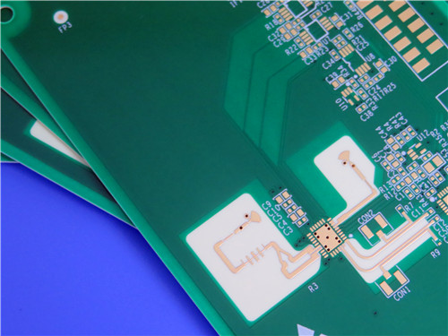
Basic PCB Specifications
| Specification | Details |
|---|---|
| Board Type | 8 layers |
| Material Type | RO4003C + FR-4 Tg 170°C |
| Solder Mask | Both sides, Green |
| Silkscreen Print | Top side, White |
| Surface Finish | ENIG (Electroless Nickel Immersion Gold) |
| Total Board Thickness | 1.5mm ± 10% |
| Board Size | 87.5mm x 40.6mm (1 PCS) |
| Minimum Hole Size | 0.2mm |
| Solder Mask Thickness | 10µm |
| Minimum Dielectric Thickness | 100µm |
| Minimum Trace Line Width | 115µm |
| Minimum Spacing | 135µm |
| Blind Vias | Yes, between L1-L2 and L7-L8 |
| Buried Vias | Yes, between L2-L7 |
| Back Drilled Vias | Yes, between L1-L6 |
| Impedance Controlled | 50 ohm, differential pairs, Top layer, 4mil / 4mil trace/gap, reference layer 2 |
| 100 ohm, differential pairs, Top layer, 5mil / 6mil trace/gap, reference layer 2 | |
| 50 ohm, single-ended, Top layer, 6mil trace, reference layer 2 | |
| Via Filling | All 0.3mm vias filled and capped per IPC 4761 Type VII |
| Edge Plating | Required |
PCB Stack-up (Component Side at Top):
| Type | Layer No. | Thickness (µm) | Specification |
|---|---|---|---|
| Copper | 1 | 45 | 18µm base copper + 25µm plating |
| RO4003C | Core | 203 | IPC-4101/24 |
| Copper | 2 | 38 | |
| FR-4 | Prepreg | 100 | IPC-4101/24 |
| Copper | 3 | 17 | |
| FR-4 S1000-2M | Core | 240 | IPC-4101/24 |
| Copper | 4 | 35 | |
| FR-4 | Prepreg | 100 | IPC-4101/24 |
| Copper | 5 | 35 | |
| FR-4 S1000-2M | Core | 240 | IPC-4101/24 |
| Copper | 6 | 17 | |
| FR-4 | Prepreg | 100 | IPC-4101/24 |
| Copper | 7 | 38 | |
| RO4003C | Core | 200 | IPC-4101/24 |
| Copper | 8 | 45 | 18µm base copper + 25µm plating |
PCB Statistics:
Components: 41
Total Pads: 73
Through Hole Pads: 35
Top SMT Pads: 26
Bottom SMT Pads: 12
Vias: 57
Nets: 6
Artwork and Standards Information
Type of Artwork Supplied: Gerber RS-274-X
Accepted Standard: IPC-Class-2
Availability: Worldwide
Typical Applications
Cellular Base Station Antennas
RF Identification Tags
Automotive Radar and Sensors
LNBs for Direct Broadcast Satellites
Computing, Communication, and Automotive Electronics
