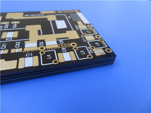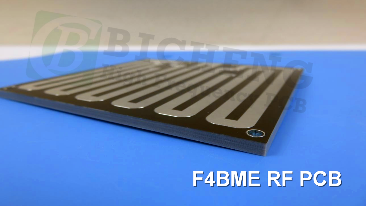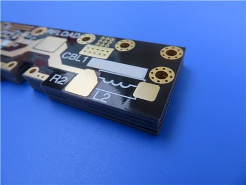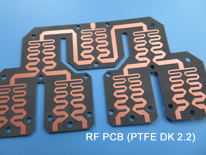
* PCBs are custom-made, picture & parameters for reference
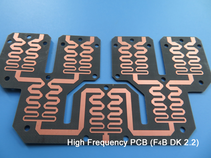
F4BME220 High-Frequency PCB PTFE DK2.2 Dual Layer Affordable RF PWB for Couplers
(Please note that Printed Circuit Boards are custom-made products; the images and specifications provided are for reference only.)
Brief Introduction
The F4BME220 PCB measures 100 x 100 mm and is designed as a dual-layer, double-sided board. This board is optimized for surface mount components and does not accommodate through-hole components. The layer stackup features a top layer composed of 35 µm (1 oz) copper, starting with 0.5 oz plating, paired with a sturdy F4BME220 core material that is 1.0 mm thick, and a corresponding 35 µm (1 oz) copper bottom layer. The surface finish is Organic Solderability Preservative (OSP), ensuring excellent soldering performance. Importantly, this PCB is not equipped with a solder mask.
PCB Specifications
| F4BME220 High Frequency PCB On DK2.2 Dual Layer Cheap RF PTFE PWB for Couplers | |
|---|---|
| PCB SIZE | 100 x 100mm = 1PCS |
| BOARD TYPE | Double sided PCB |
| Number of Layers | 2 layers |
| Surface Mount Components | YES |
| Through Hole Components | NO |
| LAYER STACKUP | copper - 35um(0.5 oz+plate) TOP layer |
| F4BME220 1.0mm | |
| copper - 35um(0.5 oz+plate) BOT Layer | |
| Minimum Trace and Space: | 10 mil / 10 mil |
| Minimum / Maximum Holes: | 0.4 mm / 0.4 mm |
| Number of Drill Holes: | 1 |
| Surface Finish | OSP |
| Final height of PCB: | 1.1 mm ±10% |
| TEST | 100% Electrical Test prior shipment |
| SERVICE AREA | Worldwide, Globally |
F4BME High-Frequency Laminates
The F4BME series laminates are crafted through a scientific formulation and rigorous pressing of fiberglass cloth, polytetrafluoroethylene (PTFE) resin, and PTFE film. The electrical performance of F4BME laminates surpasses that of F4B, mainly due to a broader range of dielectric constants, reduced dielectric loss, enhanced insulation resistance, and improved stability.
Features
Customizable DK: Options range from DK2.17 to 3.0.
Low Loss: Optimized for minimal signal loss.
Exceptional PIM Index: F4BME with RTF copper foil delivers outstanding passive intermodulation performance.
Diverse Sizes: Available in various sizes for cost efficiency.
Irradiation Resistance: Low emissions and high durability.
Commercial Viability: Suited for mass production with excellent cost-performance ratio.
Typical Applications
Microwave, radar and RF applications
Phase shifters and passive components
Power dividers, couplers, and combiners
Feed networks and phased array antennas
Satellite communications and base station antennas
Get a Quick Quote
Fill in the form below and our engineers will reply within 24 hours with technical specifications and pricing for F4BME220 High Frequency PCB (1.0mm DK2.2 OSP).
.jpg)