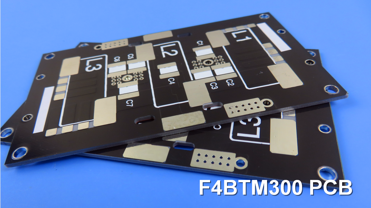
F4BTM298 10mil 2L Immersion Gold High Frequency PCB - PTFE Ceramic-Filled Substrate
(Note: Printed Circuit Boards are custom-made products. Images and parameters are for reference only.)
1. Introduction to F4BTM298 High Frequency PCB
Wangling's F4BTM298 laminates are made by scientifically formulating fiberglass cloth, nano-ceramic filling, and polytetrafluoroethylene resin, followed by strict pressing processes. The series is based on the F4BM dielectric layer, with the addition of high dielectric and low loss nano-level ceramics, resulting in higher dielectric constant, improved heat resistance, lower thermal expansion coefficient, higher insulation resistance, and better thermal conductivity, while maintaining low loss characteristics.
F4BTM298 and F4BTME298 share the same dielectric layer but use different copper foils: F4BTM is paired with ED copper foil, suitable for applications without PIM requirements, while F4BTME is paired with reverse-treated (RTF) copper foil, offering excellent PIM performance, more precise line control, and lower conductor loss.
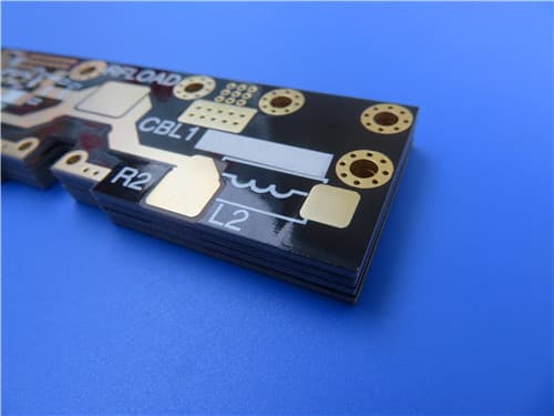
This 2-layer rigid PCB is constructed with F4BTM298 as the core material at 10mil (0.254mm) thickness, with immersion gold surface finish, black top solder mask, white top silkscreen, and 1oz copper on both sides. Its DK of 2.98 offers excellent high-frequency performance with low loss, making it ideal for demanding applications such as microwave systems, RF components, radar systems, and satellite communications.
2. Key Features of F4BTM298 PCB
Dielectric Constant (Dk): 2.98 ± 0.06 at 10GHz
Dissipation Factor (Df): 0.0018 at 10GHz
CTE x-axis: 15 ppm/°C, CTE y-axis: 16 ppm/°C, CTE z-axis: 78 ppm/°C (-55°C to 288°C)
Low Thermal Coefficient of Dk: -78 ppm/°C (-55°C to 150°C)
Moisture Absorption: ≤0.05%
Flammability: UL-94 V-0
High Thermal Conductivity: 0.42 W/(M·K) for efficient heat dissipation
Excellent PIM Performance (F4BTME version with RTF copper: ≤ -160 dBc)
Radiation resistance and low outgassing for aerospace applications
Immersion Gold Finish — Excellent solderability, corrosion resistance, and wire bondability
3. Benefits of F4BTM298 PCB
Stable DK (2.98 ± 0.06 @ 10GHz) — Consistent impedance control for high-frequency designs
Low Df (0.0018 @ 10GHz) — Excellent high-frequency performance with minimal signal loss
Nano-Ceramic Filled PTFE — Higher dielectric constant, improved heat resistance, lower CTE
Versatile DK Options — 2.98 to 3.5 available for design flexibility
Excellent PIM Performance — F4BTME variant with RTF copper offers ≤ -160 dBc
Radiation Resistance & Low Outgassing — Ideal for aerospace and defense applications
Thick and Diverse Options — Wide range of thicknesses and panel sizes for cost optimization
Commercialized, High-Volume, Cost-Effective — Proven high-volume material
4. PCB Construction Details
| Item | Specification |
|---|---|
| Base material | Wangling F4BTM298 (PTFE + Ceramic + Fiberglass) |
| Layer count | 2-layer |
| Board dimensions | 109mm x 54.5mm = 1 PCS, ±0.15mm |
| Minimum Trace/Space | 6/9 mils |
| Minimum Hole Size | 0.4mm |
| Blind vias | No |
| Finished board thickness | 0.3mm (including copper) |
| Finished Cu weight | 1 oz (35 μm / 1.4 mils) all layers |
| Via plating thickness | 20 μm |
| Surface finish | Immersion Gold |
| Top Silkscreen | White |
| Bottom Silkscreen | No |
| Top Solder Mask | Black |
| Bottom Solder Mask | No |
| 100% Electrical test | Used prior to shipment |
5. PCB Stackup (2-Layer Rigid Structure)
Layer: Copper_layer_1 (Top), Material: Copper, Thickness: 35 μm (1 oz)
Layer: Dielectric, Material: F4BTM298 Core, Thickness: 0.254 mm (10mil)
Layer: Copper_layer_2 (Bottom), Material: Copper, Thickness: 35 μm (1 oz)
6. PCB Statistics
Components: 26
Total Pads: 87
Thru Hole Pads: 49
Top SMT Pads: 38
Bottom SMT Pads: 0
Vias: 31
Nets: 2
7. Wangling F4BTM298 Material – Product Introduction
This product is made by scientifically formulating fiberglass cloth, nano-ceramic filling, and polytetrafluoroethylene resin, followed by strict pressing processes. The series is based on the F4BM dielectric layer, with the addition of high dielectric and low loss nano-level ceramics, resulting in higher dielectric constant, improved heat resistance, lower thermal expansion coefficient, higher insulation resistance, and better thermal conductivity, while maintaining low loss characteristics.
F4BTM and F4BTME share the same dielectric layer but use different copper foils: F4BTM is paired with ED copper foil, suitable for applications without PIM requirements; F4BTME is paired with reverse-treated (RTF) copper foil, offering excellent PIM performance, more precise line control, and lower conductor loss.
Key material highlights: DK 2.98~3.5可选; added ceramic for enhanced performance; F4BTME has excellent PIM performance; rich thickness options; diverse sizes for cost optimization; commercialized, high-volume, cost-effective; radiation resistance and low outgassing.
8. Features and Benefits Summary
| Feature | Benefit |
|---|---|
| DK 2.98 ± 0.06 @ 10GHz | Stable dielectric constant for consistent impedance control |
| Df 0.0018 @ 10GHz | Low loss for high-frequency RF and microwave designs |
| CTE: 15/16/78 ppm/K | Matched to copper, reliable plated through holes |
| TCDK: -78 ppm/°C | Low thermal coefficient of dielectric constant |
| Moisture Absorption ≤0.05% | Excellent stability in humid conditions |
| UL 94 V-0 | Flame retardant for safety compliance |
| Thermal Conductivity 0.42 W/M·K | Efficient heat removal for high-power applications |
| PIM ≤ -160 dBc (F4BTME) | Excellent passive intermodulation performance |
| Radiation resistance & low outgassing | Ideal for aerospace and defense applications |
| Immersion Gold finish | Excellent solderability, corrosion resistance, wire bondability |
9. F4BTM298 Typical Properties (Data Sheet)
| Property | F4BTM298 | F4BTME298 | Condition | Unit | Test Method |
|---|---|---|---|---|---|
| Electrical Properties | |||||
| Dielectric Constant (Typical) | 2.98 | 2.98 | @ 10 GHz | — | GB/T 12636-1990 / IPC-TM-650 2.5.5.5 |
| DK Tolerance | ±0.06 | ±0.06 | — | — | — |
| Dissipation Factor | 0.0018 | 0.0018 | @ 10 GHz | — | GB/T 12636-1990 |
| Dissipation Factor | 0.0023 | 0.0023 | @ 20 GHz | — | GB/T 12636-1990 |
| TCDK | -78 | -78 | -55°C ~ 150°C | ppm/°C | — |
| Volume Resistivity | ≥1×10⁷ | ≥1×10⁷ | Normal State | MΩ·cm | IPC-TM-650 |
| Surface Resistivity | ≥1×10⁶ | ≥1×10⁶ | Normal State | MΩ | IPC-TM-650 |
| Electrical Strength (Z direction) | >26 | >26 | 5KW, 500V/s | KV/mm | IPC-TM-650 2.5.6.2 |
| Breakdown Voltage (XY direction) | >34 | >34 | 5KW, 500V/s | KV | IPC-TM-650 |
| Thermal Properties | |||||
| CTE (X-axis) | 15 | 15 | -55°C ~ 288°C | ppm/°C | IPC-TM-650 2.4.41 |
| CTE (Y-axis) | 16 | 16 | -55°C ~ 288°C | ppm/°C | IPC-TM-650 2.4.41 |
| CTE (Z-axis) | 78 | 78 | -55°C ~ 288°C | ppm/°C | IPC-TM-650 2.4.41 |
| Thermal Stress | No Delamination | No Delamination | 260°C, 10s, 3 times | — | IPC-TM-650 |
| Long-Term Operating Temp | -55 ~ +260 | -55 ~ +260 | — | °C | — |
| Thermal Conductivity | 0.42 | 0.42 | Z direction | W/(M·K) | — |
| Mechanical & Physical Properties | |||||
| Peel Strength (1oz ED) | >1.6 | — | ED Copper Foil | N/mm | IPC-TM-650 2.4.8 |
| Peel Strength (1oz RTF) | — | >1.4 | RTF Copper Foil | N/mm | IPC-TM-650 2.4.8 |
| Water Absorption | ≤0.05 | ≤0.05 | 20±2°C, 24 hours | % | ASTM D570 |
| Density | 2.25 | 2.25 | Room Temperature | g/cm³ | — |
| Flammability | V-0 | V-0 | UL-94 | Grade | UL 94 |
| PIM (with RTF copper) | — | ≤-160 | — | dBc | — |
| Material Composition | |||||
| Composition | PTFE + Fiberglass + Nano-Ceramic Filling | ||||
| Copper Foil | ED Copper | RTF Copper (Reverse Treated) | F4BTM pairs with ED; F4BTME pairs with RTF | ||
10. Primary Application Areas
Microwave, RF, and radar systems
Phase shifters and feed networks
Power dividers, couplers, and combiners
Phase-sensitive antennas and phased array antennas
Satellite communications and base station antennas
RF power amplifiers and passive components
Aerospace and defense applications
11. Quality Assurance
Type of artwork supplied: Gerber RS-274-X
Accepted standard: IPC-Class-2
Availability: Worldwide
100% Electrical test prior to shipment
12. Standard Thickness, Panel Sizes & Claddings
| Parameter | Options |
|---|---|
| Standard Thickness (Total or Dielectric) | 0.254mm(10mil), 0.508mm(20mil), 0.762mm(30mil), 0.8mm, 1.0mm, 1.016mm(40mil), 1.27mm(50mil), 1.524mm(60mil), 2.0mm, 3.0mm, 4.0mm, 5.0mm, 6.0mm, 8.0mm, 10.0mm, 12.0mm (± tolerance per thickness) |
| Standard Panel Sizes | 460x610mm (18x24"), 600x500mm, 914x1220mm (36x48") — Note: ≥4.0mm not available in 914x1220mm |
| F4BTM Copper Cladding (ED) | 0.5oz (18μm), 1oz (35μm), 1.5oz (50μm), 2oz (70μm) |
| F4BTME Copper Cladding (RTF) | 0.5oz (18μm), 1oz (35μm) |
| DK Options | 2.98 ~ 3.5 (DK 2.98, 3.0, 3.2, 3.5 available) |
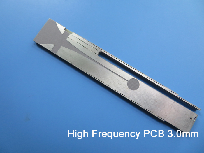
| Aluminum/Copper Base Option | F4BTM***-AL, F4BTME***-AL, F4BTM***-CU, F4BTME***-CU for shielding/heat dissipation |
| Special Options | Contact Wangling for non-standard thicknesses and custom sizes |
Get a Quick Quote
Fill in the form below and our engineers will reply within 24 hours with technical specifications and pricing for F4BTM298 10mil 2L Immersion Gold High Frequency PCB.
.jpg)
.jpg)