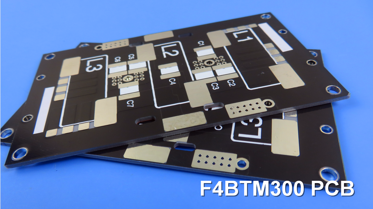
F4BTM320 High Frequency PCB 2oz Copper 1.27mm Substrates With Immersion Gold
(PCB's are custom-made products, the picture and parameters shown are just for reference)
Brief Introduction
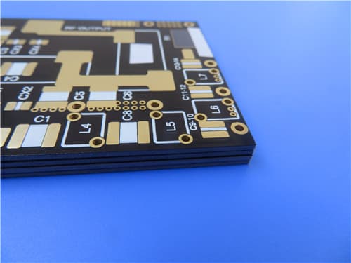
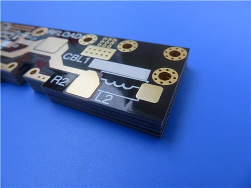
This PCB features a size of 110 mm x 76 mm and is designed as a double-sided layout with two layers. It accommodates surface mount components while excluding through-hole components. The layer stackup includes a top layer of 70 µm (2 oz) copper with starting 1 oz plating, supported by a robust F4BTM320 core material with a thickness of 1.27 mm. The bottom layer has the same copper specifications to ensure consistent performance.
The PCB allows for a minimum trace width of 5 mil and a minimum spacing of 9 mil, facilitating precise circuit design. The surface finish is immersion gold, which ensures excellent solderability and durability. Both the top and bottom sides are coated with a black solder mask, providing protection and aesthetic appeal, while white silkscreen is applied to the top side for clear labeling and identification.
PCB Specifications
| F4BTM320 High Frequency PCB 2oz Copper 1.27mm Substrates With Immersion Gold | |
|---|---|
| PCB SIZE | 110mm x 76mm = 1up |
| BOARD TYPE | Double sided PCB |
| Number of Layers | 2 layers |
| Surface Mount Components | YES |
| Through Hole Components | NO |
| LAYER STACKUP | copper - 70um(1 oz+plate) TOP layer |
| F4BTM320 - 1.27mm | |
| copper - 70um(1 oz+plate) BOT Layer | |
| Minimum Trace and Space: | 5 mil / 9 mil |
| Minimum / Maximum Holes: | 0.35 mm / 1.0 mm |
| Number of Drill Holes: | 61 |
| Surface Finish | Immersion Gold |
| Solder Mask Color: | Black (Top & Bottom) |
| Final foil external: | 2 oz |
| Final height of PCB: | 1.4 mm |
| TEST | 100% Electrical Test prior shipment |
| SERVICE AREA | Worldwide, Globally |
.jpg)
F4BTM High-Frequency Laminates
The F4BTM series laminates are made by scientifically formulating fiberglass cloth, nano-ceramic filling, and polytetrafluoroethylene resin, followed by strict pressing processes. This series is based on the F4BM dielectric layer, enhanced with high-dielectric and low-loss nano-level ceramics. These enhancements result in:
Higher dielectric constant, Improved heat resistance, Lower thermal expansion coefficient, Higher insulation resistance, Better thermal conductivity, Maintained low loss characteristics
Features & Benefits
Dielectric constant (DK) range: 2.98 - 3.5 (optional)
Addition of ceramics improves performance
Excellent PIM indicators
Thickness options ranging from 0.254 mm to 12 mm
Cost-saving properties
Suitable for commercialization and mass production
Radiation resistance
Low outgassing
Get a Quick Quote
Fill in the form below and our engineers will reply within 24 hours with technical specifications and pricing for F4BTM320 High Frequency PCB (1.27mm DK3.2 2oz Copper).
.jpg)
.jpg)